The AMD 3rd Gen Ryzen Deep Dive Review: 3700X and 3900X Raising The Bar
by Andrei Frumusanu & Gavin Bonshor on July 7, 2019 9:00 AM EST** = Old results marked were performed with the original BIOS & boost behaviour as published on 7/7.
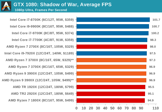
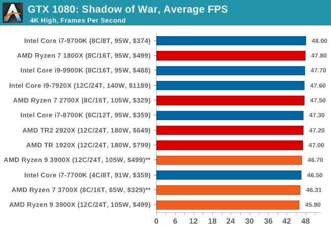
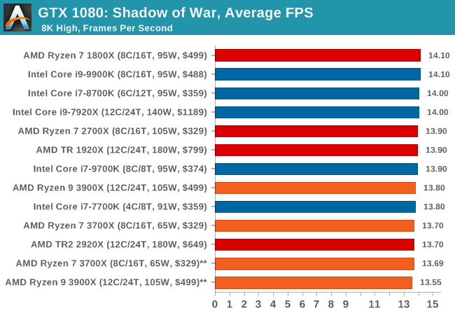
Gaming: Shadow of War
Next up is Middle-earth: Shadow of War, the sequel to Shadow of Mordor. Developed by Monolith, whose last hit was arguably F.E.A.R., Shadow of Mordor returned them to the spotlight with an innovative NPC rival generation and interaction system called the Nemesis System, along with a storyline based on J.R.R. Tolkien's legendarium, and making it work on a highly modified engine that originally powered F.E.A.R. in 2005.

Using the new LithTech Firebird engine, Shadow of War improves on the detail and complexity, and with free add-on high-resolution texture packs, offers itself as a good example of getting the most graphics out of an engine that may not be bleeding edge. Shadow of War also supports HDR (HDR10).
| AnandTech CPU Gaming 2019 Game List | ||||||||
| Game | Genre | Release | API | IGP | Low | Med | High | |
| Shadow of War | Action / RPG | Sep 2017 | DX11 | 720p Ultra | 1080p Ultra | 4K High | 8K High | |
All of our benchmark results can also be found in our benchmark engine, Bench.
| Shadow of War | IGP | Low | Medium | High |
| Average FPS | 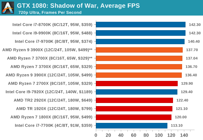 |
|
 |
 |


447 Comments
View All Comments
FireSnake - Sunday, July 7, 2019 - link
Awesome!I have been waiting for this one.
Let us start reading.
WaltC - Sunday, July 7, 2019 - link
One thing I noticed before I return to the reading is the odd bit about chipsets and memory speeds. Pretty sure the memory controller is on the CPU itself as opposed to the chipset, and I've been running DDR4-3200 XMP CL16 on my Ryzen 1 on both x370 and x470 MSI motherboards with no problems--the same DDR4 2x8 config moved from one motherboard to the next.futrtrubl - Sunday, July 7, 2019 - link
Guaranteed supported memory speeds and what overclocked memory can generally be used are two very separate things. And yes, that 3200 memory is considered an overclock for the CPU.WaltC - Sunday, July 7, 2019 - link
Right--so why tie the memory controller to the chipset? QUote: "Some motherboard vendors are advertising speeds of up to DDR4-4400 which until X570, was unheard of. X570 also marks a jump up to DDR4-3200 up from DDR4-2933 on X470, and DDR4-2667 on X370." Almost every x370, x470 motherboard produced will run DDR-4 3200 XMP ROOB. There's an obvious difference between exceeding JEDEC standards with XMP configurations and overclocking the cpu--which I've also done, but that's beside the point. Pointing out present JEDEC limitations overcome with XMP configurations is a far cry from understanding that the chipset doesn't control the memory speeds--the memory controller on the cpu is either capable of XMP settings or it isn't. Ryzen 1 is up to the task. You can also take a gander at vendor-specific motherboard ram compatibility lists to see lots of XMP 3200MHz compatibility with Ryzen 1 (and of course 2k and 3k series).edzieba - Sunday, July 7, 2019 - link
The new chipset means new boards, to which can be applied more stringent requirements of trace routing for DDR. Same as with the more stringent requirements for PCIe routing for PCIe 4.0.WaltC - Sunday, July 7, 2019 - link
OK--understood--but improved trace, imo, is mainly for PCIe4.x support with x570-- really not for DDR 3200 support, however, which has already been supported well in x370/x470 motherboards--which I know from practical experience....;) In my case it was as simple as activating the XMP profile #2 in the bios, saving the setting and rebooting. Simply was surprised to see someone tying the mem controller to the chipset! I know that the Ryzen mem controller in the CPU has been improved for Ryzen 3k series, but that has more to do with attaining much higher clocks > 3200MHz for the ram, and is relative to the CPU R 3k series, as opposed to the x570 chipset, since the mem controller isn't in the x570 chipset. All I wanted to say initially is that both DDR 4 3000 & 3200MHz have been supported all the way back to x370 boards, not by the chipset, but by the Ryzen memory controller--indeed, AMD released several AGESA versions for motherboard vendors to implement in their bioses to improve compatibility with with many different brands of memory, too.BikeDude - Sunday, July 7, 2019 - link
You mentioned 2x8GB. Try with 2x16GB and you might not be as lucky or will have to work harder to get the timing right. Motherboards that only seat two DIMMs will be noticeably easier than four DIMM motherboards.If AMD did anything to help grease the wheels, I'm sure many users will appreciate that.
FWIW, this overclocking guide has helped me a lot: https://www.techpowerup.com/review/amd-ryzen-memor...
mat9v - Sunday, July 7, 2019 - link
Does anyone know if 3900X has 3 cores for each CCX (as in 1 core in each CCX disabled) or does it have two CCX's of 4 cores and two CCX's of 2 cores?photonboy - Thursday, July 11, 2019 - link
3+3rarson - Monday, July 8, 2019 - link
WaltC, you're correct. The memory controller is part of the IO die, not the chipset. The chipset is connected to the IO die via 4 PCIe lanes.While the subsequent iterations of Ryzen have indeed improved memory support along with the new chipsets, the chipsets have nothing to do with that. I'm assuming the author is using the chipsets to delineate generations of memory improvement, but it could be just as easily (and more clearly) stated by referring to the generation of Ryzen processors.