Gen-Z Consortium Formed: Developing a New Memory Interconnect
by Ian Cutress on October 12, 2016 9:30 AM EST
Anyone tasked with handling the way data is moved around a processor deserves praise. It takes time, dedication and skill to design something that not only works appropriately and for all edge cases, but also can run at speed and seamlessly for software. The topic of interconnects has featured regularly over recent years, with cache coherent networks and unique custom designs entering both hardware released to the public as well as behind-the-scenes designs. This week sees the launch of the Gen-Z Consortium, featuring names such as ARM, Huawei, IBM, Mellanox, Micron, Samsung, SK Hynix and Xilinx, with the purpose of designing a new memory semantic fabric that focuses on the utilization of ‘on-package and storage class memory’ (HMC, phase-change, 3D XPoint etc) at the hardware level.

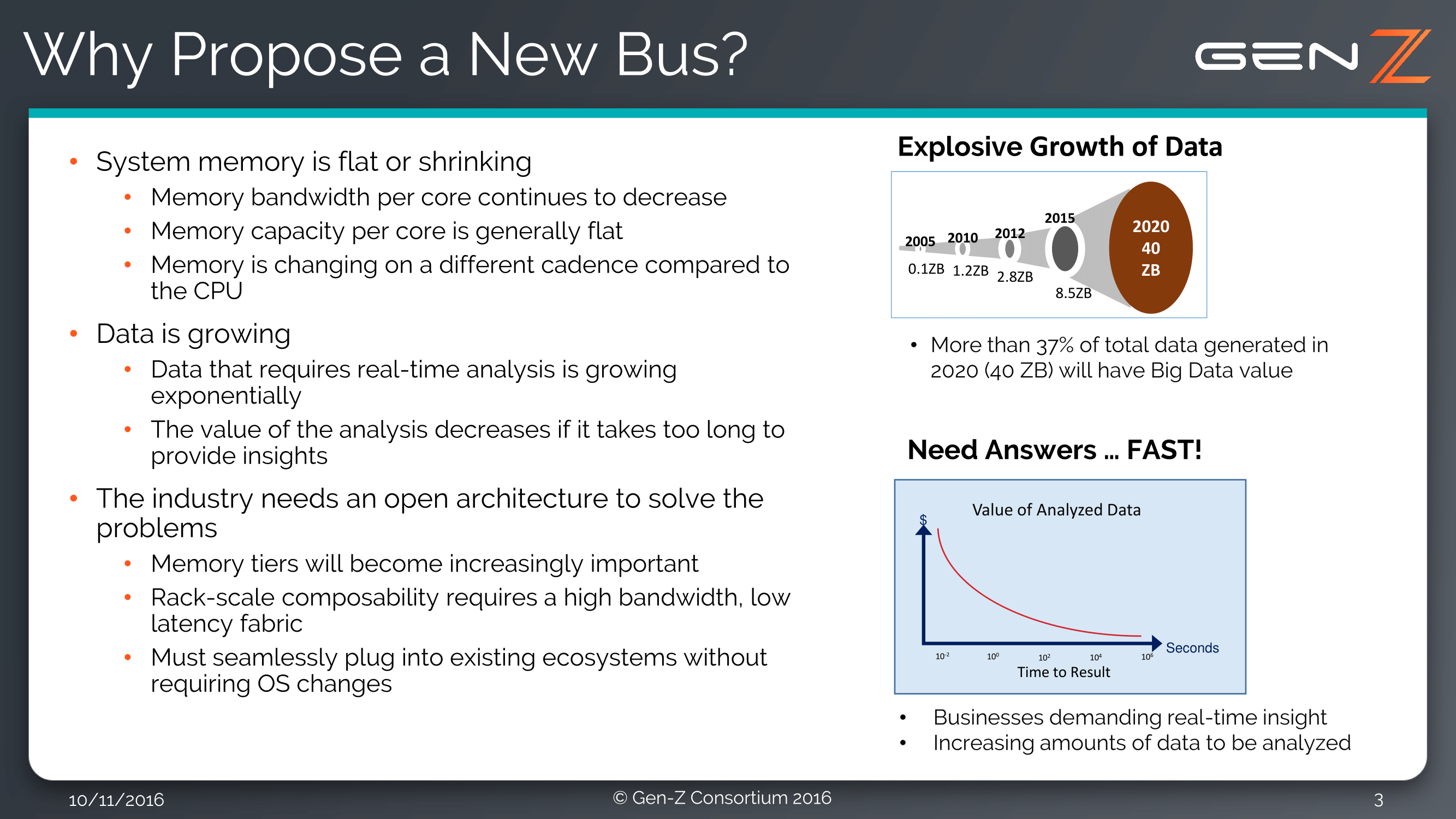
The purpose of the Consortium is the development of the interconnect, with a focus on being an open and non-proprietary standard that scales from node to rack, and free from royalties (it’s a non-profit). The interconnect will be a memory semantic fabric, handling memory operations and communications such as load/store, put/get and atomics that are typically managed by the processor and software. The issue arrives when memory is in storage class devices which are block based rather than cache line based, and thus there is an aim for a high bandwidth (>100GB/s) with low latency (sub-100ns) for load-to-use functionality.
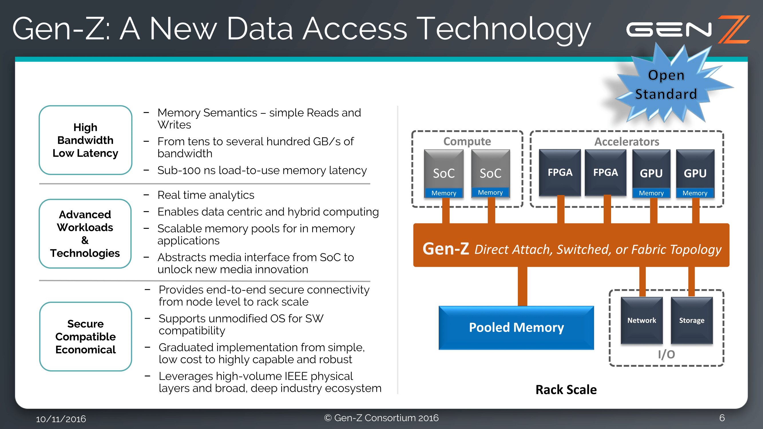
The interconnect is also aimed at offering real-time analytics, working between CPU cores, SoCs, FPGAs, GPUs, pooled memory and networked storage. There is also aims for security, as well as support via unmodified operating systems (which indicates that the new interconnect is a pure hardware design) and support within tiered memory hierarchy. Another goal is low-cost implementation, which will require working close with semiconductor manufacturers.
The Consortium consists of a number of key players designing SoCs and large scale systems:
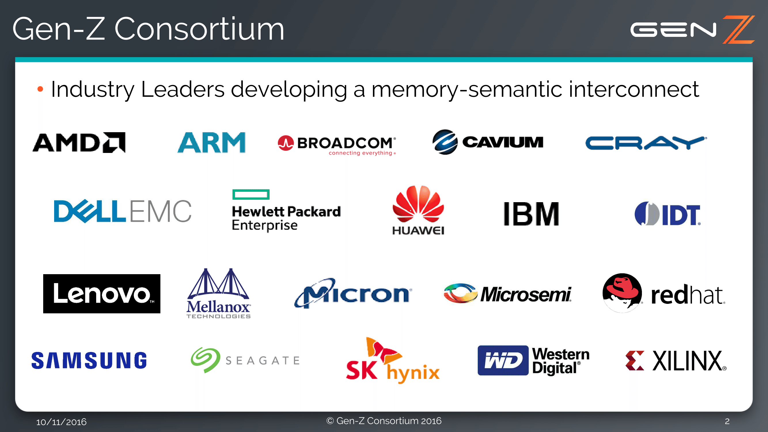
Among the IP vendors (ARM, IBM) are fabless semiconductor companies (Broadcom, Xilinx) and big enterprise players (Dell EMC, HPE, Cray for supercomputers). Any which way you cut it, it represents a lot of the industry, except one major player at least – Intel. Despite Micron in there with 3D XPoint, Intel’s own designed interconnects are under lock-and-key with patents and proprietary technology, and given how the enterprise market is moving more into accelerators and/or non-x86 architectures with a myriad of microarchitectural designs, solution providers have more options to choose from. That being said, with the goal of Gen-Z to be open and free, that doesn’t stop anyone else from actually using it and it would be argued that the ultimate goal is to promote adoption.
Despite this week being the formal announcement of the Gen-Z Consortium, it would seem that something has been brewing for a while given that the press release today has stated that the core specification covering the architecture and protocol will be finalized in late 2016. I suspect we might hear something at SuperComputing 2016 in mid-November.
Source: Gen-Z


15 Comments
View All Comments
JoeyJoJo123 - Wednesday, October 12, 2016 - link
Is it just me, or does it sound like some edgy teenagers came up with the name of this consortium? Gen-Z? Come on...XZerg - Wednesday, October 12, 2016 - link
I presumed it came from their goal to build for generation of systems where Zettabytes of storage is as standard...ddriver - Wednesday, October 12, 2016 - link
It came from the goal to have a silly moniker for everything that can otherwise be referred to using standard terminology.Noremacam - Wednesday, October 12, 2016 - link
That's because Generations A-Y were complete failures.eddieobscurant - Wednesday, October 12, 2016 - link
weird name coincidence with the upcoming samsung's z-ssdszodiacfml - Wednesday, October 12, 2016 - link
Interesting. Before posting this comment I went to check the latest news on fiber optics which lasted for an hour of reading. I was surprised by my lack of knowledge on the latest fiber news. Anandtech should include such.I discovered that the optical techniques I know 10 years ago still applies and to which I know that fiber has virtually infinite bandwidth as a student. Yet, seeing the current bandwidth possible on a single fiber amazed me a lot. It also brought me to dark fiber which is intriguing.
Going back to the article, attached memory makes sense. I have seen comments from users that Ethernet networking is approaching memory speeds. Though far from the truth and it does tell that DRAM can be on a remote location.
The only concern is that HBM might be become mainstream (lower cost and increased density, performance) and then DRAM modules might not be cost effective anymore while non-volatile becomes cheaper and faster.
DanNeely - Wednesday, October 12, 2016 - link
Ethernet approaching memory bandwidths is a rather optimistic claim at best. Dual channel DDR4 can hit ~30GB/sec or 240gbps in commodity hardware vs 10gbps ethernet still being almost entirely limited to enterprise servers (which are probably equipped with quadcore memory controllers for 2x the bandwidth quoted above) and the 100gbps standard being AFAIK almost entirely limited to very high end data center network backbones and the like at present.GPUs are an order of magnitude higher, the Tesla P100 his 720GBps/5,760gbps with the consumer centric 1080 GTX at 320GBps/2560gbps.
The fastest undersea data cables can hit multiple terabits per second smoking even GPU memory busses; but at the cost of complexity and prices orders of magnitude beyond ethernet.
http://www.corsair.com/en-us/blog/2014/september/d...
Yojimbo - Wednesday, October 12, 2016 - link
Gen-Z uses an Ethernet physical layer.http://genzconsortium.org/faq/gen-z-technology/#17
zodiacfml - Thursday, October 13, 2016 - link
Thanks for the link.zodiacfml - Thursday, October 13, 2016 - link
- I don't know why some users mention that but the idea comparing memory bandwidth and networking is still interesting.- The Tesla P100 uses HBM2. Such technology will scale even higher. I feel that it might happen in SoCs soon.
- A single fiber has vast bandwidth. If limited by cost and present technology, adding more cables quickly solves the problem.