Intel's Process Roadmap to 2025: with 4nm, 3nm, 20A and 18A?!
by Dr. Ian Cutress on July 26, 2021 5:00 PM ESTCustomers Customers Customers
As a roadmap announcement today, the focus isn’t so much on the customers but on the technology. Because Intel is moving into a phase where it expects its IFS offerings to compete against the established players, it has to consider its disclosures with respect to both its internal use and any external interest, which is a new concept for the company – at least on this scale compared to its previous foundry efforts.
Intel CEO Pat Gelsinger, in the company’s Q3 financial call last week, was keen to point out that they already have a large hyperscaler customer signed up for their next generation packaging technology, however today there would appear to also be another customer in the mix. Now we assume that Intel’s Foundry Services is talking to 100s of chip companies, big and small, but it doesn’t take much to sign an NDA to start to talk – what will be interesting is when customers start making commitments to using Intel’s facilities, and if any of those are volume orders.
As part of the announcement today, Intel held a little bit back from us, saying that they are saving some of the details specifically for the event that is going on as we publish this piece. All we know is that our draft press release has a big yellow bar that says ‘[customer news]’ on it, right next to Intel’s 20A process node details.
For reference, Intel 20A is a 2024 technology using first generation Gate-All-Around transistors, marketed as RibbonFETs, as well as backside power delivery, marketed as PowerVias. At this time Intel expects to have second/third-generation EMIB available as well as fourth-generation Foveros Direct. So if a customer is already committing to Intel 20A, there’s going to be a lot of potential here.
When the announcement is made, we will update this news article.
To conclude, Intel maintains that these roadmaps will showcase a clear path to process performance leadership* by 2025. It’s a tall order, and the company has to execute better than it has in recent memory - but that’s kind of why the company has rehired a number of former Intel experts and fellows in research, product design, and execution.
*as measured by performance per watt at iso-power
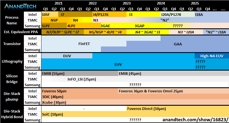
Here's a secondary comparison chart (compared to the one on page one) with all three main foundry offerings listed in each of the main segments that Intel has discussed today.


326 Comments
View All Comments
nandnandnand - Monday, July 26, 2021 - link
https://hplusmagazine.com/2011/11/01/femtocomputin...GauravMunjal - Monday, July 26, 2021 - link
First, it's femtometer, then picometer. Second, given that most atoms are bigger than 1 angstrom, I doubt we'll ever need a smaller unit.martinpw - Monday, July 26, 2021 - link
Given that the number bears no relationship to feature size, I think we will one day be in the interesting position that the headline number used to name the process will actually be smaller than the spacing between silicon atoms (which would happen at 5A)Unashamed_unoriginal_username_x86 - Monday, July 26, 2021 - link
Nano: 10^-9Pico: 10^-12
Femto: 10^-15
I agree with your second point though
ishould - Monday, July 26, 2021 - link
Nuh uhcolaman - Monday, July 26, 2021 - link
Lol no, pico is larger than femto. Double check before you call someone out.Kevin G - Monday, July 26, 2021 - link
Marketing and switching to picometers makes the mantissa that much larger than the previous nanometer figures. Going from 3 nm to 2000 pm makes the later seem much much larger to those who don't know metric suffixes that well.Realistically you'd think that there marketing departments would do when they switched from microns to nanometers: the first few sub-micron generations were expressed as a decimal micron: 0.8 um, 0.65 um, then they switches to nanometers. Main point here is that there is a firm bottom limit to how low these numbers can go.
There is also the problem that we're up against atomic size limitations. A single silicon atom is ~118 pm wide. The difference between the 20A process and 18A process if they fully represented physical characteristics would simply be two Si atom's width.
mode_13h - Monday, July 26, 2021 - link
This only matters if they actually deliver. Intel has a gaping credibility problem. The bar is high for them to convince customers & investors they've actually fixed the root problems behind prior delays.KAlmquist - Monday, July 26, 2021 - link
If they deliver on this roadmap, that will do a lot to fix their credibility issues. Their tick-tock strategy had the following schedule:32nm 2010
22nm 2012
14nm 2014
10nm 2016
4nm 2018
2nm 2020
Things went a little off the rails with 14nm, which was about six months late. 10nm was nominally delivered in 2018 (two years late), but given that Rocket Lake, released earlier this year, used 14nm, I don't think you can really claim that 10nm was fully there prior to this year. Intel now plans to deliver a new process every year, but the changes between are smaller, so that's similar to their previous goal of a new process every two years. So you add five years to the original tick-tock road map, giving:
10nm 2021
4nm 2023
2nm 2025
That's ambitious. Time will tell whether they can pull it off.
mode_13h - Monday, July 26, 2021 - link
I'd give them 10 nm in 2019. Volumes were low, but Ice Lake was a real product (unlike Canon Lake). 10 nm SF reached comparable volumes in 2020.