Intel's Process Roadmap to 2025: with 4nm, 3nm, 20A and 18A?!
by Dr. Ian Cutress on July 26, 2021 5:00 PM ESTCustomers Customers Customers
As a roadmap announcement today, the focus isn’t so much on the customers but on the technology. Because Intel is moving into a phase where it expects its IFS offerings to compete against the established players, it has to consider its disclosures with respect to both its internal use and any external interest, which is a new concept for the company – at least on this scale compared to its previous foundry efforts.
Intel CEO Pat Gelsinger, in the company’s Q3 financial call last week, was keen to point out that they already have a large hyperscaler customer signed up for their next generation packaging technology, however today there would appear to also be another customer in the mix. Now we assume that Intel’s Foundry Services is talking to 100s of chip companies, big and small, but it doesn’t take much to sign an NDA to start to talk – what will be interesting is when customers start making commitments to using Intel’s facilities, and if any of those are volume orders.
As part of the announcement today, Intel held a little bit back from us, saying that they are saving some of the details specifically for the event that is going on as we publish this piece. All we know is that our draft press release has a big yellow bar that says ‘[customer news]’ on it, right next to Intel’s 20A process node details.
For reference, Intel 20A is a 2024 technology using first generation Gate-All-Around transistors, marketed as RibbonFETs, as well as backside power delivery, marketed as PowerVias. At this time Intel expects to have second/third-generation EMIB available as well as fourth-generation Foveros Direct. So if a customer is already committing to Intel 20A, there’s going to be a lot of potential here.
When the announcement is made, we will update this news article.
To conclude, Intel maintains that these roadmaps will showcase a clear path to process performance leadership* by 2025. It’s a tall order, and the company has to execute better than it has in recent memory - but that’s kind of why the company has rehired a number of former Intel experts and fellows in research, product design, and execution.
*as measured by performance per watt at iso-power
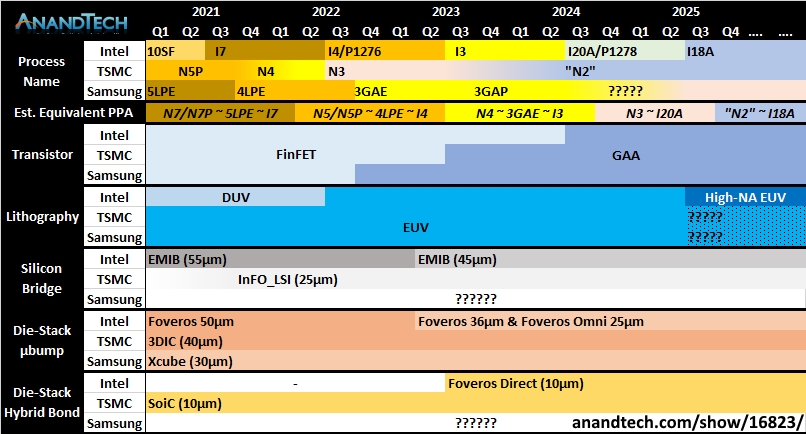
Here's a secondary comparison chart (compared to the one on page one) with all three main foundry offerings listed in each of the main segments that Intel has discussed today.


326 Comments
View All Comments
svan1971 - Monday, July 26, 2021 - link
why not just say 1nm in 2025 ? If your gonna lie, lie big or go homeishould - Monday, July 26, 2021 - link
Well, then Intel would win all silicon, game over, ggWaltC - Monday, July 26, 2021 - link
You know, Intel can't even hit 7nm yet--so there's no sense in discussing anything at all beyond that. He who makes the best products shall win the game--not so hard to understand, is it, Intel? I haven't seen an interesting architecture out of Intel yet! AMD has flashed by you as if you are sitting still...but hey--you are just sitting still, aren't you, Intel? Products talk--BS walks.RanFodar - Monday, July 26, 2021 - link
What kind of crap is this? You know Intel acknowledges their own faults now, and they're trying to remedy that with the first of these announcements. This node scheming is only for the purpose of realinging with the industry— and they're being more honest for that sake. Why not hold them to account to see if they're getting more and more competitive by the next few years?DigitalFreak - Monday, July 26, 2021 - link
Re-aligning with the industry? They're just making things up.persondb - Monday, July 26, 2021 - link
What are they making up? Their 10nm/7nm node is in the end about equal to TSMC and Samsung 7nmmode_13h - Monday, July 26, 2021 - link
Intel has been about as transparent as a brick wall. Their disclosures of schedule slip have been the bare minimum required by their customers and SEC reporting requirements. To this day, we still have zero visibility into exactly what went wrong. They've listed a bunch of leadership and organizational changes, but without insight into the root problems, it just amounts to: "trust us this time, for realz!"> Why not hold them to account to see if they're getting more and more competitive
> by the next few years?
Been there, done that. They've published similar roadmaps in the past, and they turned out to be worth less than the bits they were printed on.
Many years late, Intel did manage to get 10 nm products into end users' hands, followed by 10 nm SFF. So, they haven't lost *all* credibility. We can expect them to deliver on most of their promises *eventually*. It's mainly just a question of which decade.
Kevin G - Tuesday, July 27, 2021 - link
Intel hasn't disclosed what went wrong but looking at what the other fabs have done it should be pretty evident: they went with EUV sooner and were not as aggressive pursuing peak density. Intel's 10 nm process was a quad pass, self aligned schema that is seemingly too complex for mass production. The super fin and enhanced super fin advancements sacrificed that absolute density in favor of getting a working node.EUV is a great reset on as it reduces the need for multi-pass layers. This is also why Intel does have a legit chance in surpassing the other foundries with high-NA by securing these next generation ASML machines before their competitors. If the competition doesn't have these same tools at the same time as Intel, it is a clear technological advantage. The real question is how much money did it take to secure that deal.
mode_13h - Wednesday, July 28, 2021 - link
> they went with EUV soonerUh, no. I thought they were *late* to the EUV party and got themselves in a position of having to wait in line to get EUV machines. The article is consistent with this.
> were not as aggressive pursuing peak density.
I heard their 10 nm was too high-density, and that was part of the problem. From the chart on page 1, it's certainly claimed to be higher-density than TSMC 7 nm.
> EUV is a great reset on as it reduces the need for multi-pass layers.
I thought EUV requires more passes, which is one reason it's more expensive.
Spunjji - Thursday, July 29, 2021 - link
@mode_13h - I think Kevin G meant Intel's *competitors* went with EUV sooner, not Intel - hence also them not aggressively pursuing peak density, which is not something Intel could be accused of...EUV reduces the number of passes required, because less (or no) multi-patterning is required to reach the same density as a process using DUV. The problem you're likely thinking of is that EUV machines are still in a state where each pass through them is slower than through a DUV machine due to relatively weak beam intensity, and the masks have to be handled with greater care (no pellicles) and replaced more often.
Presumably Intel thought they would be better off sweating existing known-good assets than trying to figure out how to integrate relatively experimental tech into an entirely new workflow. They lost that bet.