AMD Zen 2 Microarchitecture Analysis: Ryzen 3000 and EPYC Rome
by Dr. Ian Cutress on June 10, 2019 7:22 PM EST- Posted in
- CPUs
- AMD
- Ryzen
- EPYC
- Infinity Fabric
- PCIe 4.0
- Zen 2
- Rome
- Ryzen 3000
- Ryzen 3rd Gen
Cache and Infinity Fabric
If it hasn’t been hammered in already, the big change in the cache is the L1 instruction cache which has been reduced from 64 KB to 32 KB, but the associativity has increased from 4-way to 8-way. This change enabled AMD to increase the size of the micro-op cache from 2K entry to 4K entry, and AMD felt that this gave a better performance balance with how modern workloads are evolving.
The L1-D cache is still 32KB 8-way, while the L2 cache is still 512KB 8-way. The L3 cache, which is a non-inclusive cache (compared to the L2 inclusive cache), has now doubled in size to 16 MB per core complex, up from 8 MB. AMD manages its L3 by sharing a 16MB block per CCX, rather than enabling access to any L3 from any core.
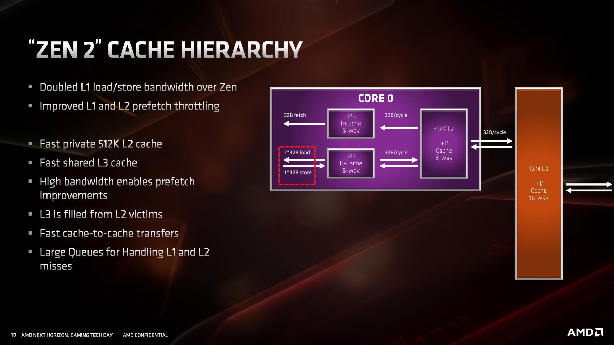
Because of the increase in size of the L3, latency has increased slightly. L1 is still 4-cycle, L2 is still 12-cycle, but L3 has increased from ~35 cycle to ~40 cycle (this is a characteristic of larger caches, they end up being slightly slower latency; it’s an interesting trade off to measure). AMD has stated that it has increased the size of the queues handling L1 and L2 misses, although hasn’t elaborated as to how big they now are.
Infinity Fabric
With the move to Zen 2, we also move to the second generation of Infinity Fabric. One of the major updates with IF2 is the support of PCIe 4.0, and thus the increase of the bus width from 256-bit to 512-bit.
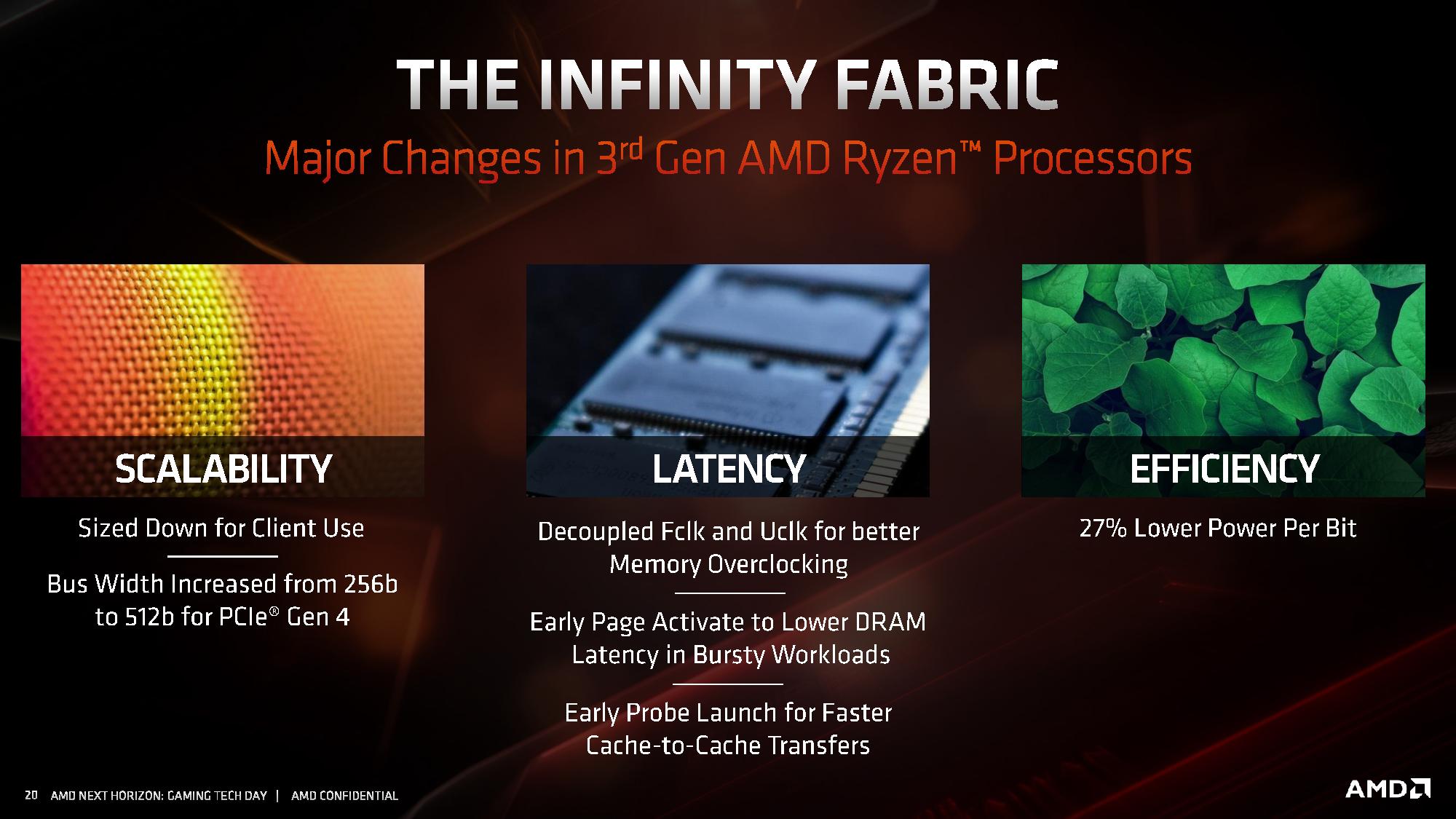
Overall efficiency of IF2 has improved 27% according to AMD, leading to a lower power per bit. As we move to more IF links in EPYC, this will become very important as data is transferred from chiplet to IO die.
One of the features of IF2 is that the clock has been decoupled from the main DRAM clock. In Zen and Zen+, the IF frequency was coupled to the DRAM frequency, which led to some interesting scenarios where the memory could go a lot faster but the limitations in the IF meant that they were both limited by the lock-step nature of the clock. For Zen 2, AMD has introduced ratios to the IF2, enabling a 1:1 normal ratio or a 2:1 ratio that reduces the IF2 clock in half.
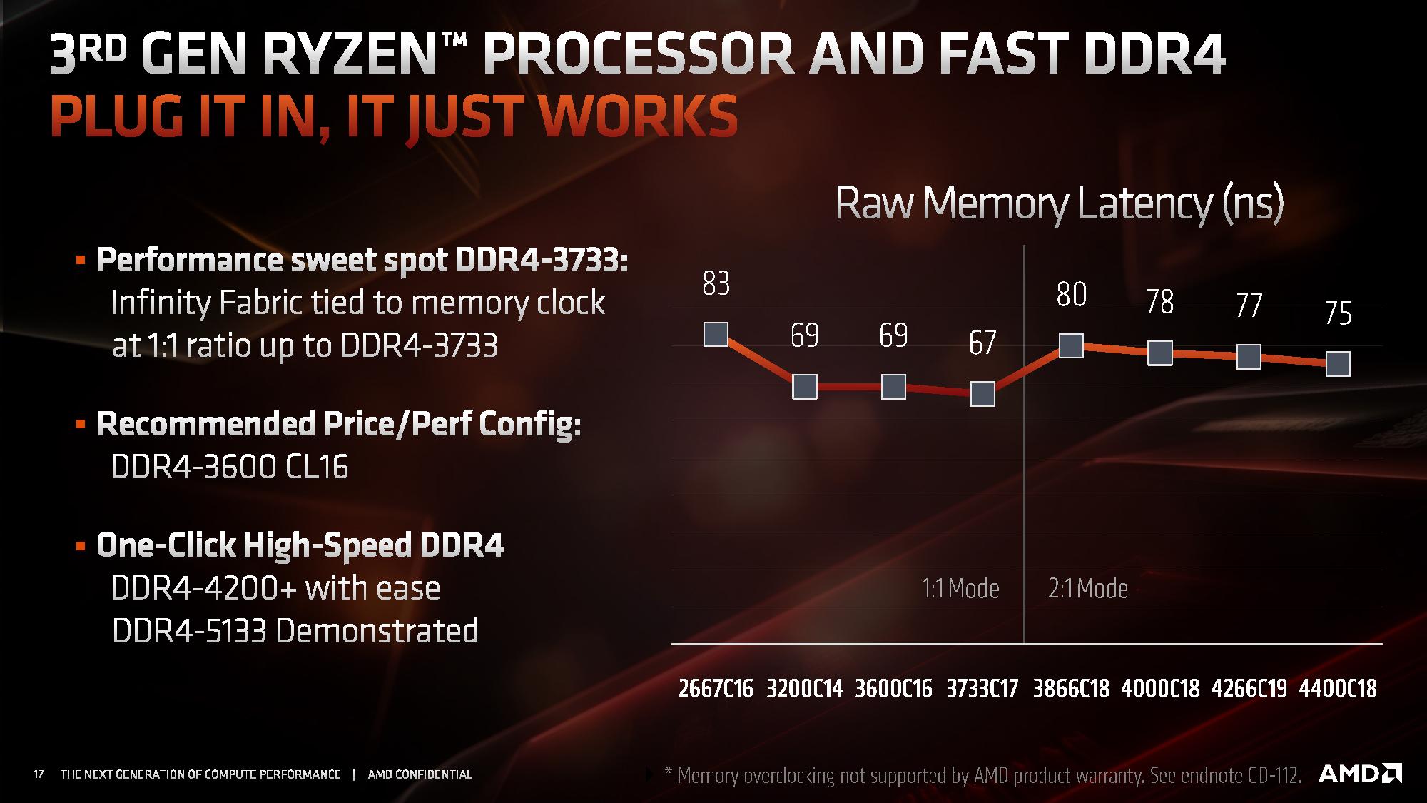
This ratio should automatically come into play around DDR4-3600 or DDR4-3800, but it does mean that IF2 clock does reduce in half, which has a knock on effect with respect to bandwidth. It should be noted that even if the DRAM frequency is high, having a slower IF frequency will likely limit the raw performance gain from that faster memory. AMD recommends keeping the ratio at a 1:1 around DDR4-3600, and instead optimizing sub-timings at that speed.


216 Comments
View All Comments
Walkeer - Thursday, June 13, 2019 - link
Superb analysis, thanks a lot @Ian! very excited to have the 3900x at home alreadyFreckledTrout - Thursday, June 13, 2019 - link
Reading over the Zen2 microarchitecture article Im left wondering if the Windows scheduler improvements are making use of a new unmentioned RDPID feature in Zen2 to determine where threads are placed?cooker358 - Thursday, June 13, 2019 - link
感谢分享!Gastec - Thursday, June 13, 2019 - link
I too am curious about the latencies, particularly between the chiplets. With the clock selection down to 2 ns and Windows' 10 hopefully improved thread allocation (filling a CCX, then the next one before jumping to the 2nd chiplet) latencies should be lower. We'll just have to wait for honest extensive testing and reviews to be done. You were not planning on buying these CPUs on release day or even worse, pre-ordering them, were you? :)jamescox - Sunday, June 16, 2019 - link
I expect the CCX to CCX latencies to be very good. There is no memory clock on the cpu chiplet, so the two on die CCX almost certainly communicate at cpu clock rather than memory clock as in Zen 1. It isn’t the same as Intel’s mesh network, but AMD’s solution will have better L3 latency within the CCX compared to Intel. Intel’s mesh network seems to be terrible for power consumption. Intel’s ring bus didn’t scale to enough cores. For their 18 core chip (if I am remembering right), they actually had 3 separate ring buses. The mesh network is obviously not workable across multiple chiplets, so it will be interesting to see what Intel does.For the chiplet to chiplet latency, they have more than doubled the infinity fabric serdes clock with the higher than PCIe 4.0 speeds. It seems that the internal IF clock is also around doubled. It was operating at actual memory clock in Sen 1 which was half the DDR rate. They seem to be running the internal IF clock the same as the DDR rate with the option to drop back to half DDR rate. So if you are running DDR 3200, the IF clock may actually be 3200 instead of 1600 as it would be in Zen 1. If you re overclocking to DDR 4000 or something, then it may need to drop down to 2000 for the internal IF clock. If this is the way it is set up, then they may have an option to explicitly set the divider, but it is probably going to not be stable past 3.7 GHz or so. The IO die is 14 nm global foundries, so that seems like a reasonable limitation.
The CCX to CCX latency should be less important as the OS and software is better optimized for the architecture. There was quite a few cases on Zen 1 of applications performing significantly better on Linux compared to windows due to the scheduler. Most applications can be optimized a bit for this architecture also. The problem is fine grained shared memory between threads on different CCX. It generally a good idea to reduce that anyway since locking can be detrimental to performance. With Zen 2, I think application level optimizations are probably going to be a lot less necessary anyway, but a lot of the early issues were probably caused by bad multi-threaded programming. This type of architecture isn’t going away. Intel can’t compete with Epyc 2 with a monolithic die. Epyc 2 will be around 1000 square mm of silicon total. Intel can’t scale core count without moving to something similar.
frshi - Friday, June 14, 2019 - link
@Ian Cutress What about 2x16GB sticks compared to 4x8GB? I remember Zen and Zen+ were kinda picky when using 4 sticks. Any change to that on Zen 2?RAINFIRE - Saturday, June 15, 2019 - link
Yeah - I'm curious. Can anyone speak to the (4 x 32GB) memory that Ryzen 3000 and x570 boards are supposed to support?Holliday75 - Wednesday, June 19, 2019 - link
IF reviewers have samples at this time they are under an NDA until July 7th. Only unconfirmed leaks can provide that kind of info and its super early. A lot of these types of issues won't be known until they go retail.AdrianMel - Sunday, June 16, 2019 - link
I would like these AMD chips to be used on laptops. Would be a breakthrough in terms of computing power, lower consumption. I think if a HBM2 or higher memory is integrated into the processor, I think it will double the computing power. Ar fi de studiat si o implementare a 2 porturi superiare thnic vechiului expresscard 54 in care sa putem introduce in laptopuri 2 placi videojamescox - Sunday, June 16, 2019 - link
Everyone keeps bringing up HBM for cpus as if it is magical in some manner. HBM can provide high bandwidth, but it is still DRAM. He latency isn’t that great, so it isn’t really that useful as a cpu cache. If you are trying to run AVX512 code across a bunch of CPU cores, then maybe you could use the bandwidth. If you have code that can use that level of parallelism, then it will almost certainly run much more efficiently on an actual gpu. I didn’t think that expanding AVX to 512-bits was a good idea. There isn’t too much difference from a cpu perspective between 1 512-bit instruction and 2 256-bit instructions. The registers are wider, but they can have many more smaller registers that are specified in the ISA by using existing register renaming techniques. At 14 nm, the 512-bit units seem to take too much space and consume too much power. They may be more easily doable in 7 nm or below eventually, but they may still have issues running at cpu core clocks. If you have to run it at half clock (which is about where gpus are vs. cpus) then you have lost the advantage of going double the width anyway. IMO, the AVX 512 instructions were Intel’s failed attempt (Xeon Phi seems to have been a disappointment) at making a cpu act like a gpu. They have basically given that up and are now designing an actual gpu.I went off in a bit of a tangent there, but HBM really isn’t that useful for a cpu cache. It isn’t going to be that low of latency; so it would not increase single thread performance much compared to stuff actually designed to be a low latency cache. The next generations form AMD May start using active silicon interposers, but I would doubt that they would use HBM. The interposer is most likely to be used in place of the IO die. They could place all of the large transistors needed for driving off die interfaces (reason why IO doesn’t scale well) in the active interposer. They could then stack 7 nm chips on top of the active interposer for the actual logic. Cache scales very well which is why AMD can do a $200 chip with 32 MB of L3 cache and a $500 chip with 64 MB of L3. Intel 14 nm chips top out at 38.5 MB, mostly for high priced Xeon chips. With an active interposer, they could, for example) make something like 4 or 8 memory controller chips with large SRAM caches on 7 nm while using the active interposer for the IO drivers. Many different configurations are possible with an active interposer, so it is hard to speculate. Placing HBM on the IO interposer, as the AdoredTV guy has speculated, doesn’t sound like a great idea. Two stacks of HBM deliver 512 GB/s, which would take around 10 IF links to transfer to the CPU chiplets. That would be a massive waste of power. If they do use HBM for cpu chiplets, you would want to connect it directly to the cpu chiplet; you would place the a cpu chiplet and HBM stack on the same interposer. That would have some latency advantage, but mostly for large systems like Epyc.