AMD Zen 2 Microarchitecture Analysis: Ryzen 3000 and EPYC Rome
by Dr. Ian Cutress on June 10, 2019 7:22 PM EST- Posted in
- CPUs
- AMD
- Ryzen
- EPYC
- Infinity Fabric
- PCIe 4.0
- Zen 2
- Rome
- Ryzen 3000
- Ryzen 3rd Gen
Building a core like Zen 2 requires more than just building a core. The interplay between the core, the SoC design, and then the platform requires different internal teams to come together to create a level of synergy that working separately lacks. What AMD has done with the chiplet design and Zen 2 shows great promise, not only in taking advantage of smaller process nodes, but also driving one path on the future of compute.
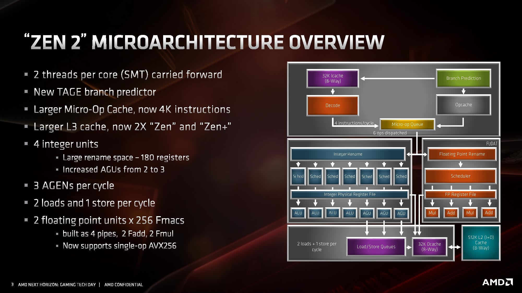
When going down a process node, the main advantages are lower power. That can be taken in a few ways: lower power for operation at the same performance, or more power budget to do more. We see this with core designs over time: as more power budget is opened or different units within the core get more efficient, that extra power is used to drive cores wider, hopefully increasing raw instruction rate. It’s not an easy equation to solve, as there are many trade-offs: one such example in the Zen 2 core is the relationship between the reduced L1 I-cache that has allowed AMD to double the micro-op cache, which overall AMD expects to help with performance and power. Going into the minutae of what might be possible, at least at a high level, is like playing with Lego for these engineers.
All that being said, Zen 2 looks a lot like Zen. It is part of the same family, which means it looks very similar. What AMD has done with the platform, enabling PCIe 4.0, and putting the design in place to rid the server processors of the NUMA-like environment is going to help AMD in the long run. The outlook is good for AMD here, depending on how high it can drive the frequency of the server parts, but Zen 2 plus Rome is going to remove a good number of questions that customers on the fence had about Zen.
Overall AMD has quoted a +15% core performance improvement with Zen 2 over Zen+. With the core changes, at a high level, that certainly looks feasible. Users focused on performance will love the new 16-core Ryzen 9 3950X, while the processor seems nice an efficient at 105W, so it will be interesting so see what happens at lower power. We're also anticipating a very strong Rome launch here over the next few months, especially with features like double FP performance and QoS, and the raw multithreading performance of 64 cores is going to be an interesting disruptor to the market, especially if priced effectively. We’ll be getting the hardware on hand here soon to present our findings when the processors are launched on July 7th.


216 Comments
View All Comments
JohnLook - Monday, June 10, 2019 - link
@Ian Cutress Are you sure the Io dies are on TSMC's 14 & 12 nm processes ?all info so far was that they were on GloFo's 14 nm ...
Ian Cutress - Monday, June 10, 2019 - link
Sorry, glofo 14 and 12. Matisse IO die is Glofo 12nm. We triple confirmed.JohnLook - Monday, June 10, 2019 - link
Thanks :-)scineram - Tuesday, June 11, 2019 - link
It still says Epyc is TSMC.John_M - Tuesday, June 11, 2019 - link
It would be nice if the article was updated as not everyone reads the comments section and AnandTech articles do often get cited in Wikipedia articles.Smell This - Wednesday, June 12, 2019 - link
I feel safe in saying that Wiki-Dom will be right on it . . .;-)
So __ those little white lines are the Infinity Scalable Data Fabric (SDF) and the Infinity Scalable Control Fabric (SCF), connecting "Core" chiplets to the I/O core.
"The SDF might have dozens of connecting points hooking together things such as PCIe PHYs, memory controllers, USB hub, and the various computing and execution units."
"The SDF is a superset of what was previously HyperTransport. The SCF is a complementary plane that handles the transmission ..."
https://en.wikichip.org/wiki/amd/infinity_fabric
Of course, I counted them (rolling eyes at myself), and determined there were 32 connecting a single core chiplet to the I/O core. I'm smelling a rational relationship between those 32, and other such stuff. Are the number of IF links a proprietary secret to AMD?
Yah know? It would be a nice 'get' if a tech writer interviewed someone in that former Sea Micro bunch, and spilled a few beans . . .
Smell This - Wednesday, June 12, 2019 - link
Might be 36 ... LOL
Smell This - Wednesday, June 12, 2019 - link
Could be 42- or 46 IF links on the right(I'll stop obsessing)
sweetca - Thursday, June 13, 2019 - link
I don't understand anything you said 🙂Smell This - Sunday, June 16, 2019 - link
I was (am) trolling Ian/AT for a **Deep(er) Dive** on the Infinity Fabric -- its past, and its future. The EPYC Rome processors have 8 "Core" chiplets connecting to the I/O core. Right? Those 'little white lines' (32- to 46?) from each chiplet, presumably, scale to ... infinity?AMD purchased SeaMicro 7 years ago as the "Freedom Fabric" platform was developed. Initially the SM15000 'stitched' together 512 compute cores, 160 gigabits of I/O networking and 5+ petabytes of storage to form a 'very-high-density server.'
And then . . . they went dark.
https://www.anandtech.com/show/9170/amd-exits-dens...
(see the last comment on that link)