Examining Intel's Ice Lake Processors: Taking a Bite of the Sunny Cove Microarchitecture
by Dr. Ian Cutress on July 30, 2019 9:30 AM EST- Posted in
- CPUs
- Intel
- 10nm
- Microarchitecture
- Ice Lake
- Project Athena
- Sunny Cove
- Gen11
Thunderbolt 3: Now on the CPU*
One of the big failures of the Thunderbolt technology since its inception has been its adoption beyond that Apple ecosystem. In order to use it, both the host and the device needed TB controllers supplied by Intel. It wasn’t until Thunderbolt 3 started to use USB Type-C, and Thunderbolt 3 having enough bandwidth to support external graphics solutions, that we started to see the number of available devices start to pick up. The issue still remains that the host and device need an expensive Intel-only controller, but the ecosystem was starting to become more receptive to its uses.
With Ice Lake, that gets another step easier.
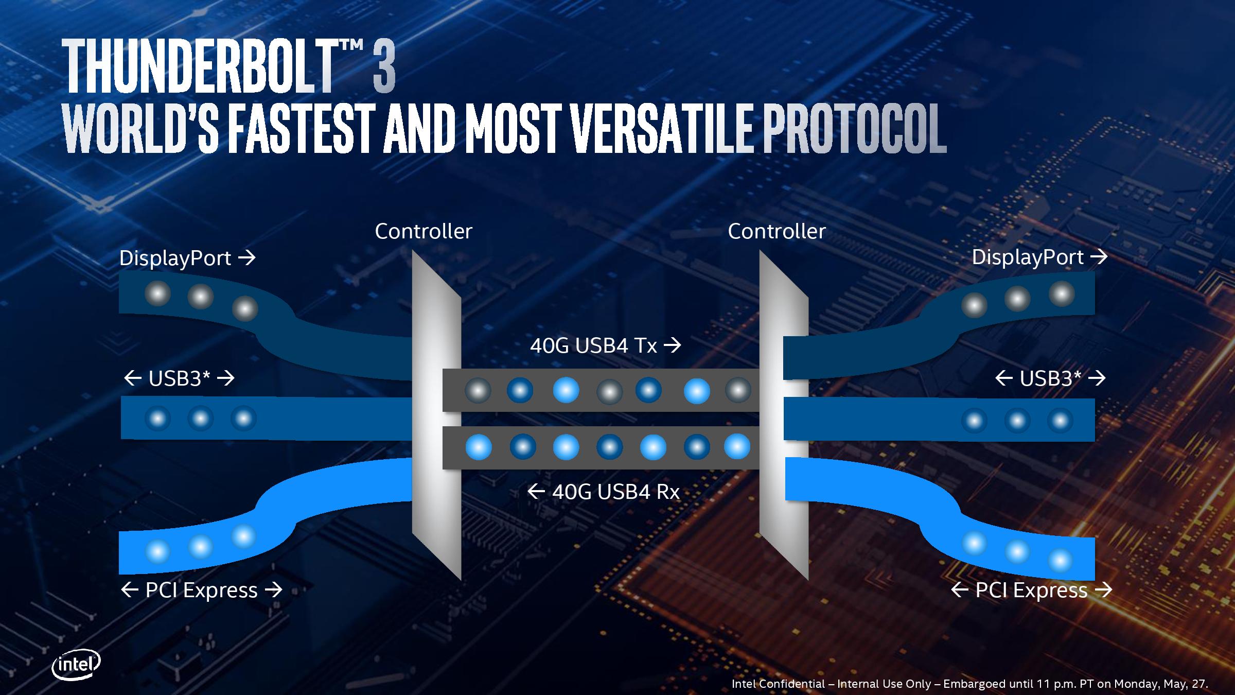
Rather than bundle TB3 support into the chipset, Intel has integrated it on the die of Ice Lake, and it takes up a sizable amount of space. Each Ice Lake CPU can support up to four TB3 ports, with each TB3 port getting a full PCIe 3.0 x4 root complex link internally for full bandwidth. (For those keeping count, it means Ice Lake technically has 32 PCIe 3.0 lanes total).
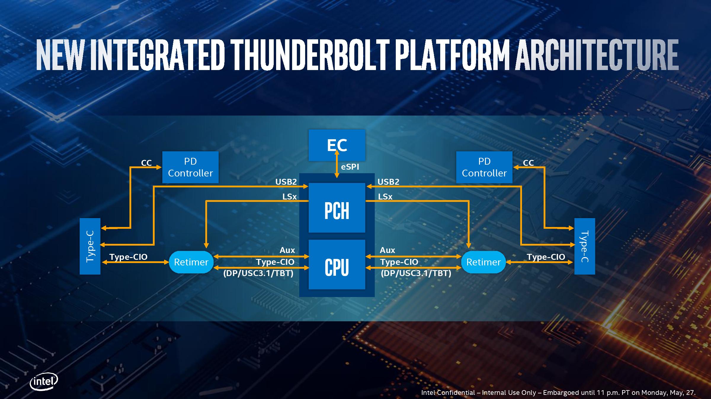
Intel has made it so each side of the CPU can support two TB3 links direct from the processor. There is still some communication back and forth with the chipset (PCH), as the Type-C ports need to have USB modes implemented. It’s worth noting that TB3 can’t be directly used out of the box, however.
Out of the four ports, it will be highly OEM dependent on how many of those will actually make it into the designs – it’s not as simple as just having the CPU in the system, but other chips (redrivers) are needed to support the USB Type-C connector. Power delivery too requires extra circuitry, which costs money. So while Intel advertises TB3 support on Ice Lake, it still needs something extra from the OEMs. Intel states that a retimer for the integrated solution is only half the size compared to the ones needed with the TB3 external chips, as well as supporting two TB3 ports per retimer, therefore halving the number of retimers needed.
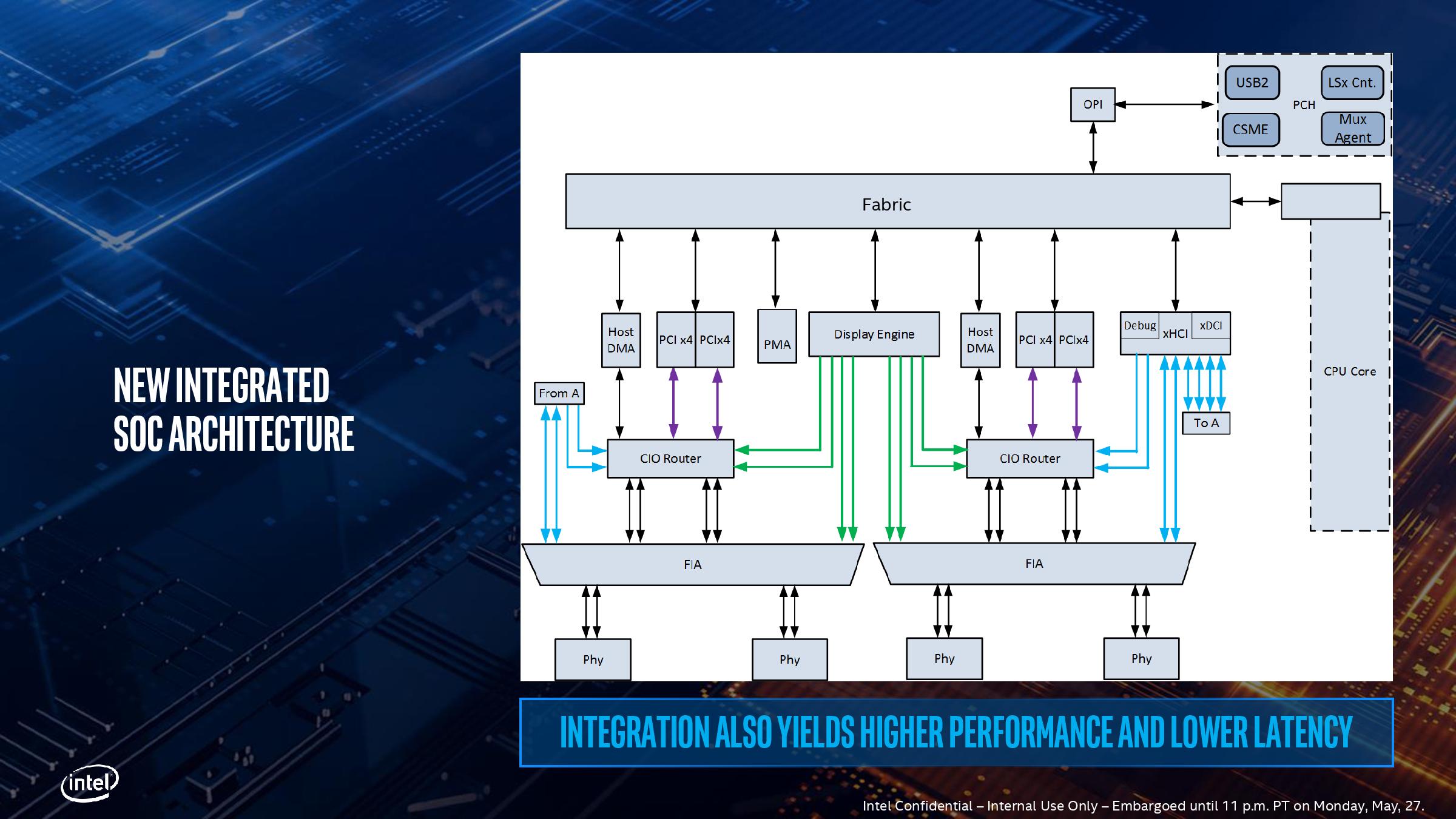
Here’s a more detailed schematic, showing the complexities of adding in TB3 into a chip, with the four PCIe x4 complexes shown moving out to each of the individual PHYs at the bottom, and connected back into the main SoC interconnect fabric. The display engine also has to control what mode the TB3 ports are in, and what signals are being sent. Wake up times for TB3 in this fashion, according to Intel, are actually slightly longer compared to a controller implementation, because the SoC is so tightly integrated. This sounds somewhat counterintuitive, given that the requisite hardware blocks are now closer together, but it all comes down to power domains – in a separate chip design, each segment has a separate domain with individual power up/down states. In an integrated SoC, Intel has unified the power domains to reduce complexity and die area, which means that more careful management is required but latency ultimately increases a little bit.
The other upside to the tightly coupled integration is that Intel stated that this method of TB3 is a lot more power efficient that current external chip implementations. However they wouldn’t comment on the exact power draw of the TB3 block on the chip as it corresponds to the full TDP of the design, especially in relation to localized thermal density (Intel was initially very confused by my question on this, ultimately saying that the power per bit was lower compared to the external chip, so overall system power was lower – they seemed more interested in discussing system power over chip power). Intel did state that the difference between an idle and a fully used link was 300 mW, which suggests that if all four links are in play, we’re looking at 1.2 W. When asked, Intel stated that there are three different power delivery domains within the TB3 block depending on the logic, that the system uses integrated voltage regulation, and the TB3 region has an internal power rail that is shared with some of the internal logic of the CPU. This has implications when it comes to time-to-wake and idle power, but Intel believes it has found a good balance.
Regarding USB4 support, Intel stated that it is in the design, and they are USB4 compliant at this point, but there might be changes and/or bugs which stop it from being completely certified further down the line. Intel said that it ultimately comes down to the device side of the specification, although they have put as much in as they were able given the time constraints of the design. They hope to be certified, but it’s not a guarantee yet.
Depending on who you speak to, this isn’t Intel’s first crack at putting TB3 into CPU silicon: the chip that Intel never wants to talk about, Cannon Lake, supposedly also had an early TB3 design built inside that never worked. But Intel is confident in its Ice Lake implementation, especially with supporting four ports. I wouldn’t be surprised if this comes to desktop when Intel releases its first generation 10nm desktop processors.
*The asterisk in the title of this page is because you still need external hardware in order to enable TB3.


107 Comments
View All Comments
The_Assimilator - Wednesday, July 31, 2019 - link
Getting Thunderbolt on-die is huge for adoption. While I doubt many laptop manufacturers will enable more than a single TB port, desktop is an entirely different kettle of fish.umano - Wednesday, July 31, 2019 - link
I am afraid but I cannot consider 4 cores cpu as premiumKhenglish - Wednesday, July 31, 2019 - link
This honestly is looking like the worst architecture refresh since Prescott. IPC increases are getting almost completely washed out by loss in frequency. I wonder if this would have happened if Ice Lake came out on 14nm. Is the clock loss from uArch changes, process change, or a mix of both?Performance of an individual transistor has been decreasing since 45nm, but overall circuit performance kept improving due to interconnect capacitance decreasing at a faster rate at every node change. It looks like at Intel 10nm, and TSMC 7nm that this is no longer true, with transistor performance dropping off a cliff faster than interconnect capacitance reduction. 5nm and 3nm should be possible, but will anyone want to use them?
Sivar - Wednesday, July 31, 2019 - link
"...with a turbo frequency up to 4.1 GHz"This is the highest number I have come across for the new 10th generation processors, and according to SemiAccurate (which is accurate more often than not), this is likely not an error.
If this value is close to desktop CPU limitations, the low clock speed all but erases the 18% IPC advantage -- an estimate likely based on a first-gen Skylake.
Granted, the wattage values are low, so higher-wattage units should run at least a bit faster.
Farfolomew - Wednesday, July 31, 2019 - link
I’m a bit confused by the naming scheme. Ian, you say: “The only way to distinguish between the two is that Ice Lake has a G in the SKU and Comet Lake has a U”But that’s not what’s posted in several places throughout the article. The ICL processors are named Core iX-nnnnGn where CML are Core iX-nnnnnU. Comet lake is using 5 digits and Ice Lake only 4 (1000 vs 10000 series).
Is this a typo or will ICL be 1000-series Core chips?
name99 - Wednesday, July 31, 2019 - link
Regarding AI on the desktop. The place where desktop AI will shine is NLP. NLP has lagged behind vision for a while, but has acquired new potency with The Transformer. It will take time for this to be productized, but we should ultimately see vastly superior translation (text and speech), spelling and grammar correction, decent sentiment analysis while typing, even better search.Of course this requires productization. Google’s agenda is to do this in the cloud. MS’ agenda I have no idea (they still have sub-optimal desktop search). So probably Apple will be first to turn this into mainstream products.
Relevant to this article is that I don’t know the extent to which instructions and micro-architectures optimized for CNNs are still great for The Transformer (and the even newer and rather superior Transformer-XL published just a few months ago). This may all be a long time happening on the desktop if INTC optimized too much purely for vision, and it takes another of their 7 years to turnaround and update direction...
croc - Thursday, August 1, 2019 - link
It seems that Ice Lake / Sunny Cove will have hardware fixes for Spectre and Meltdown. I would like to see some more information on this, such as how much speed gain, whether the patch is predictive (so as to block ALL such OOE / BP exploits) etc.MDD1963 - Thursday, August 1, 2019 - link
A month or so ago, we heard a few rumors that the CPUs were ahead ~18% in IPC (I see that number again in this article), but are down ~20+% in clock speed.... ; it would be nice to see at least one or two performance metrics/comparisons on a shipped product. :)isthisavailable - Thursday, August 1, 2019 - link
Unlike Ryzen mobile, intel’s “upto” 64 EUs part will probably only ship in like 2 laptops. Therefore amd has more designs in my book. I don’t understand people who buy expensive 4K laptops with intel integrated gfx which can’t even render windows 10 ui smoothly.Looking forward to Zen2 + navi based 7nm APU.
Bulat Ziganshin - Thursday, August 1, 2019 - link
> it can be very effective: a dual core system with AVX-512 outscored a 16-core system running AVX2 (AVX-256).it's obviously wrong - since ice lake has only one avx-512 block but two avx2 blocks, it's not much faster in avx-512 mode compared to avx2 mode
the only mention of HEDT cpus at the page linked is "At a score of 4519, it beats a full 18-core Core i9-7980XE processor running in non-AVX mode". Since AVX-512 can process 16 32-bit numbers in a single operation, no wonder that a single avx-512 core matches 16 scalar cores