Intel's Architecture Day 2018: The Future of Core, Intel GPUs, 10nm, and Hybrid x86
by Dr. Ian Cutress on December 12, 2018 9:00 AM EST- Posted in
- CPUs
- Memory
- Intel
- GPUs
- DRAM
- Architecture
- Microarchitecture
- Xe
It has been hard to miss the fact that Intel has been vacuuming up a lot of industry talent, which brings with them a lot of experience. Renduchintala, Koduri, Keller, Hook, and Carvill, are just to name a few. This new crew has decided to break Intel out of its shell for the first time in a while, holding the first in a new tradition of Intel Architecture Days. Through the five hours of presentations, Intel lifted the lid on the CPU core roadmaps through 2021, the next generation of integrated graphics, the future of Intel’s graphics business, new chips built on 3D packaging technologies, and even parts of the microarchitecture for the 2019 consumer processors. In other words, it's many of the things we've been missing out on for years. And now that Intel is once again holding these kinds of disclosures, there’s a lot to dig in to.
Contents List
Intel covered a good amount of ground at the Architecture Day, which we’ve split into the following categories:
- The CPU Core and Atom Roadmaps, on 10nm
- The Sunny Cove Microarchitecture
- The Next Generation Gen11 Graphics
- Intel Demonstrates Sunny Cove and Gen11 Graphics
- Beyond Gen11 Graphics: Announcing the Xe Graphics Brand
- 3D Packaging with FOVEROS
- Intel’s first Fovoros and first Hybrid x86 CPU: Core plus Atom in 7 W on 10nm
- Ice Lake 10nm Xeon
- Intel Made Something Really Funny: Q&A with Raja, Jim, and Murthy
The CPU Core Roadmaps
It is common for companies like Intel to ask members of the press what they enjoy about announcements from Intel, Intel’s competitors, or other companies in the industry. One of answers I will never tire of saying is ‘roadmaps’. The roadmap is a simple document but it enables a company to explain part of its future plans in a very easy to understand way. It shows to the press, to customers, and to partners, that the company has a vision beyond the next product and that it expects to deliver at a rough cadence, hopefully with some markers on expected performance additions or improvements. Roadmaps are rarely taken as set in stone either, with most people understanding that they have an element of fuzziness depending on external factors.
To that end, I’ve been requesting Intel to show roadmaps for years. They used to be common place, but ever since Skylake, it has kind of dried up. In recent months Intel has shown rough datacentre roadmaps, with Cascade Lake, Cooper Lake, and Ice Lake and the next few generations. But for the Core family it has been somewhat more difficult. Depending on which analyst you talk to, a good number will point to some of the Skylake derivatives as being holding points while the issues with 10nm have been sorted out. But nonetheless, all we tend to hear about is the faint whisper of a codename potentially, which doesn’t mean much.
So imagine my delight when we get not one roadmap from Intel on CPUs, but two. Intel gave us both the Core architecture roadmap and the Atom architecture roadmap for the next few generations.
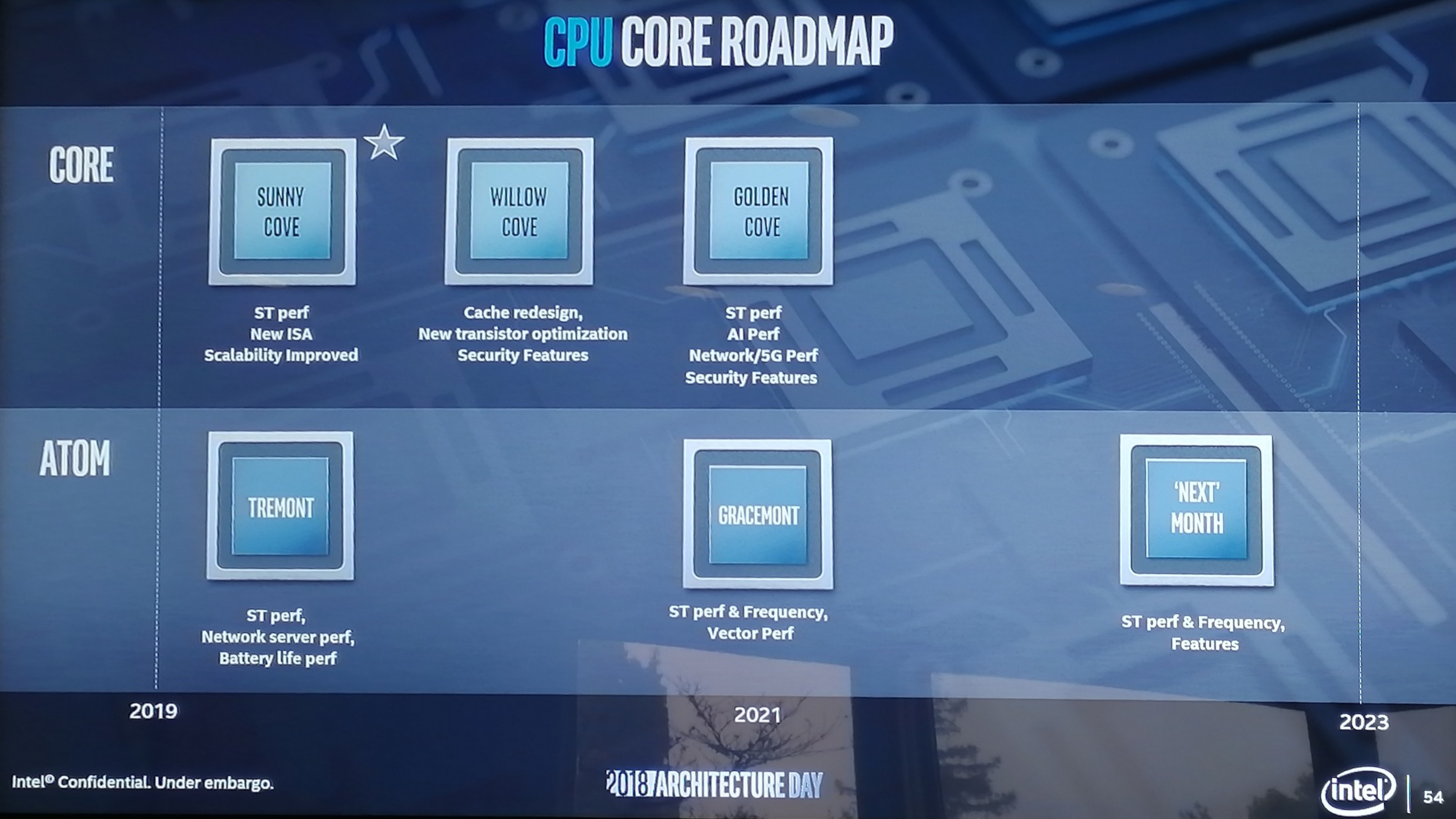
For the high performance Core architecture, Intel lists three new codenames over the next three years. To be very clear here, these are the codenames for the individual core microarchitecture, not the chip, which is an important departure from how Intel has previously done things.
Sunny Cove, built on 10nm, will come to market in 2019 and offer increased single-threaded performance, new instructions, and ‘improved scalability’. Intel went into more detail about the Sunny Cove microarchitecture, which is in the next part of this article. To avoid doubt, Sunny Cove will have AVX-512. We believe that these cores, when paired with Gen11 graphics, will be called Ice Lake.
Willow Cove looks like it will be a 2020 core design, most likely also on 10nm. Intel lists the highlights here as a cache redesign (which might mean L1/L2 adjustments), new transistor optimizations (manufacturing based), and additional security features, likely referring to further enhancements from new classes of side-channel attacks.
Golden Cove rounds out the trio, and is firmly in that 2021 segment in the graph. Process node here is a question mark, but we’re likely to see it on 10nm and or 7nm. Golden Cove is where Intel adds another slice of the serious pie onto its plate, with an increase in single threaded performance, a focus on AI performance, and potential networking and AI additions to the core design. Security features also look like they get a boost.
| Intel Core Microarchitecture Roadmap | |||
| Core Name | Year | Process Node | Improvements |
| Skylake | 2015 | 14 nm | Single Threaded Performance Lower Power Other Optimizations |
| Kaby Lake | 2016 | 14 nm+ | Frequency |
| Coffee Lake | 2017 | 14 nm++ | Frequency |
| Coffee Refresh | 2018 | 14 nm++ | Frequency |
| Sunny Cove | 2019 | 10 nm | Single Threaded Performance New Instructions Improved Scalability |
| Willow Cove | 2020 ? | 10 nm ? | Cache Redesign New Transistor Optimization Security Features |
| Golden Cove | 2021 ? | 7 / 10 nm ? | Single Threaded Performance AI Performance Networking / 5G Performance Security Features |
The lower-powered Atom microarchitecture roadmap is on a slower cadence than the Core microarchitecture, which is not surprising given its history. Seeing as how Atom has to fit into a range of devices, we’re expecting there to be a wide range in capabilities, especially from the SoC side.
The upcoming microarchitecture for 2019 is called Tremont, which focuses on single threaded performance increases, battery life increases, and network server performance. Based on some of the designs later in this article, we think that this will be a 10nm design.
Following Tremont will be Gracemont, which Intel lists as a 2021 product. As Atom is designed to continually push both the performance at the high-end of its capabilities and the efficiency at the low-end, Intel lists that Gracemont will have additional single threaded performance and a focus on increased frequency. This will be combined with additional vector performance, which likely means that Atom will get some wider vector units or support new vector instructions.
Beyond this will be a future ‘mont’ core (and not month as listed in the image). Here Intel is spitballing what this new 2023 core might have, for which the general listing of performance, frequency and features is there.
| Intel Atom Microarchitecture Roadmap | |||
| Year | Process | Improvements | |
| Goldmont | 2016 | 14 nm | Higher Performance Cryptography Features |
| Goldmont Plus | 2017 | 14 nm | Branch Prediction More Execution Larger Load/Store Buffers More Cache |
| - | 2018 | - | - |
| Tremont | 2019 | 10 nm ? | Single Threaded Performance Network Server Performance Battery Life |
| - | 2020 | - | - |
| Gracemont | 2021 | 10 nm ? | Single Threaded Performance Frequency Vector Performance |
| - | 2022 | - | - |
| 'Next Mont' | 2023 | ? | Single Threaded Performance Frequency 'Features' |
As stated above, these are just the microarchitecture names. The actual chips these cores are in will likely have different names, which means a Lake name for the Core microarchitecture. At the event, Intel stated that Ice Lake would have Sunny Cove cores in it, for example.
Another aspect to Intel’s presentations was that future microarchitectures are likely to be uncoupled from any process technologies. In order to build some resiliency into the company’s product line moving forward, both Raja Koduri and Dr. Murthy Renduchintala explained that future microarchitectures will not be process dependent, and the latest products will come to market on the best process technologies available at the time. As a result we’re likely to see some of the Core designs straddle different manufacturing technologies.
Intel also went into a bit of detail on microarchitecture of Sunny Cove.


148 Comments
View All Comments
ajc9988 - Thursday, December 13, 2018 - link
https://www.anandtech.com/show/13445/tsmc-first-7n...Risk production is in Q2 next year. And Mass is listed by Q2 2020 for 5nm.
https://www.extremetech.com/mobile/278800-tsmc-exp...
So, I was a bit off by the estimate for volume being 2020, but you were off on when risk production starts. Meanwhile, 7nm+ is already confirmed for AMD on Zen3, as the benefits of 5nm+ don't outweigh the costs associated moving to the process for AMD. This is why it is thought AMD will skip 5nm and try 3nm when available. But, TSMC has not said when 3nm will be available, while Samsung is saying 3nm in 2021:
https://semiengineering.com/big-trouble-at-3nm/
https://www.cdrinfo.com/d7/content/samsung-details...
http://www.semimedia.cc/?p=2524 (saying TSMC 3nm in 2022/23)
I cannot find the article speculating Apple will be the first customer on 5nm EUV and when ATM.
HStewart - Thursday, December 13, 2018 - link
"Nodes are marketing jargon"Exactly - it reminds me the frequence wars back in P4 days. But if you look closely at Intel's plan - I am no chip designer - even though I did take Micro-code Enginnering classes in College, but Foveros is revolutionary design - I thought EMiB was amazing, but to do that in 3rd diminsion is awesome - maybe one they could even stack cores that way - instead huge chip monsters.
But a nm rating by vendor 1 does not nm rating by vendor 2 - what underneath makes the different - Intel is extremely smart to decouple nm process from actual archexture. If you notice by Intel archiexture Intel has more improvements in core archiexture over next 3 years - this is because they are not limited by process (nm)
ajc9988 - Friday, December 14, 2018 - link
EMIB was not revolutionary and neither is foveros. They are incremental steps and existing competing solutions are available and have been for some time. Not only that, it will only be used on select products with eventual spread to the stack.Go to the second page of comments and see my links there. I think you will find those quite interesting. Not only that, this has been done with HBM for years now. If you look at AMD's research, almost half a decade ago, they were studying optimal topologies for active interposers. They found only 1-10% of the area was needed for the logic routing of an active interposer. Moving a couple I/O items onto the active interposer just is an extension. In fact, you can put those components on a spread out interposer between the above chiplets that sit on the interposer, but would need to plan on the heat dissipation or having so low a heat that it doesn't need sinked.
Considering lack of details of what is on the active interposer or timeline for mainstream, HEDT, and server markets, I will assume those won't see this until 2020, with the first products being mobile in nature.
In fact, Intel this summer gave AIB patents to DARPA to try to control what tech is used for chiplets moving forward, proposing that be used. AMD proposed a routing logic protocol which would be agnostic to routing on the chiplets itself, increasing compatibility moving forward.
Now, if EMIB is so "revolutionary", do the Intel with AMD GPUs seem revolutionary? Because that is the only product that comes to mind that uses it. Those chips are Hyades Canyon and Crimson Canyon. It isn't that dissimilar to other data fabric uses.
So far, on disintegration of chip components, AMD's Epyc 2 is getting there. It literally uses just cores and the interconnect for the chiplet (for this description, I am including cache with the cores, but when latency is reduced with active interposers, I do expect an L3 or L4 or higher caches or integrated memory on package to be introduced external to the "core" chiplet moving forward). From there, we could see the I/O elements further subdivided, we could see GPU, modems, etc. But all of this has been planned since the 2000s, so I don't see anything new other than the culmination around the same time other alternative solutions are being offered, just that the cost/benefit analysis has not tipped in its favor just yet, but should in the next year or so, which should bring many more designs to the forefront. Here is a presentation slideshow discussing the state of current 2.5D and 3D packaging. After review, I'd like to hear if you still think EMIB and Foveros are "revolutionary." Don't get me wrong, they are an incremental success and should be honored as such. But revolutionary is too strong a word for incremental process. Overall, it changes nothing and is the culmination of a lot of work over a decade by numerous companies and engineers. Even competing solutions can act as inspiration for another company moving forward and Intel's engineers read the whitepapers and published peer reviewed articles on the cutting edge, just like everyone else in the industry.
As to you saying Intel is smart to do it, they haven't done it except in silicon in labs and in papers, unless talking the EMIB with Intel CPU. AMD has a product line, Epyc 2, where the I/O is made at GF on 14nm and the chiplet is made on 7nm TSMC with greater pitch disparity. Intel hasn't really removed the components off the core chip yet into each separate element. ARM is considering something similar, and this is the logical progression for the custom designed chips for RISC V moving forward (may take a little longer, less well funded).
Meanwhile, this doesn't seem to stack high performance cores on high performance cores. The problem of thermals cooking the chip are too great to solve at this moment, which is why low power components are being placed relative to the higher performance (read as higher heat producing) components. Nothing wrong with that, it makes sense.
But, what doesn't make sense is your flowering lavish praise on Intel for something that doesn't seem all that extraordinary in light of the industry as a whole.
johannesburgel - Thursday, December 13, 2018 - link
People keep saying the same thing about Intel's 14nm process, which is allegedly equal or better than other fab's 10nm processes. But AMD currently makes products on 14nm and 12 nm processes which Intel apparently can't build on its own 14nm process. For example there is still no 32-core Xeon while AMD will soon ship 64 core EPYCs and lots of other companies have 32/48/64 core designs on the market. Many Intel CPUs have much higher effective TDPs than their equivalent AMD CPUs.So pardon me if I am not willing to simply believe in all this "Intel's process is better in the end" talk.
HStewart - Thursday, December 13, 2018 - link
But intel's single core performance is better than AMD's single core performance. Just because AMD glues 8 core cpus together does not make them betterIcehawk - Thursday, December 13, 2018 - link
Node isn't even close to everything.Rudde - Wednesday, December 12, 2018 - link
Gen 11 graphics in desktops is said to reach double the performance of gen 9.5 desktop graphics. 2W Atoms have half the max frequency of desktop graphics and half or three quarters of the execution units. The 7W custom hybrid processor has the full amount of execution units. I'd guess it has half the frequency of it's desktop counterpart to stay within power limits. This would put it at the same performance as 9.5-gen desktop parts, or actually at 30% higher performance.Think about that. 80% single thread performance compared to current high-end desktop processors (my quick est.) and 130% graphics performance. That's a solid notebook for web browsing, legacy programs and even for light gaming. All that at a power budget of a tablet.
If I were to bet, I'd bet on a MS Surface Book.
Spunjji - Thursday, December 13, 2018 - link
Now that would be nice!Intel999 - Wednesday, December 12, 2018 - link
Keep in mind that 3DXpoint came to market three years past the initial promise from Intel. 10nm will be appearing 4 or 5 years late depending on when volume production materializes.Chances are that this 3D stacked promise for late 2019 will show up around 2022.
I'm seeing alot of fellow Intel fanboys show a semblance of confidence that has been absent in recent months and rightfully so.
Let's all hope Intel can deliver this time on time.
ajc9988 - Wednesday, December 12, 2018 - link
I disagree on worrying about Intel with the active interposer. They use passive interposers for the mesh on HEDT and Xeons and Xeon Phi (since around 2014) for years now. The 22nm active interposer is to fill out fab time due to pushing chipsets back to plants that were going to be shut down due to moving to 10nm, which never came.Meanwhile, AMD did a 2017 cost analysis saying that below 32nm would cost as much as a monolithic die, so it seems they are waiting due to cost, not on technical capability.
Either way, Intel doesn't hit 7nm until 2021, around the time 3nm may be ready at TSMC, if they go to 3nm within a year of volume 5nm products expected in 2020. That means Intel will never regain the process lead moving forward in any significant way, unless everyone else gets stuck on cobalt integration.