ASML's First High-NA EUV Litho Scanner Arrives At Intel [UPDATED]
by Anton Shilov on January 5, 2024 7:30 AM EST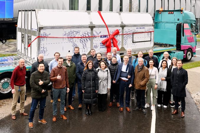
Update 1/5/2024: Intel Oregon announced on Thursday that it has received its shipment of ASML's first-generation Twinscan EXE:5000 High-NA EUV lithography scanner. The two companies will start assembly process of the machine shortly and then Intel will start its High-NA learning curve with the aim to insert the technology into mass production with their post-18A node.
The best way to start the year. 🎊
— Intel News (@intelnews) January 4, 2024
Intel Oregon welcomes major components of @ASMLcompany’s first shipped High-NA EUV technology to help enable the continued and relentless pursuit of Moore’s Law.
Learn more: https://t.co/a5RVr1iWLX pic.twitter.com/NYEUozN4iM
The original story follows as below:
Originally Published: 12/21/2023
ASML on Thursday said that it had shipped its pilot High-NA EUV scanner to Intel. The Twinscan EXE:5000 extreme ultraviolet (EUV) scanner is AMSL's very first High-NA scanner, and it has eagerly been awaited by Intel, who first placed an order for the machine back in 2018. Intel will be using the new machine to experiment with High-NA EUV before it deploys commercial grade Twinscan EXE:5200 tool for high-volume manufacturing (HVM) sometime in 2025. The announcement represents a major industry milestone that will have an impact not only on Intel, but eventually on the other leading-edge fabs as well.
"We are shipping the first High NA system and announced this in a social media post today," a spokesperson for ASML said. "It goes to Intel as planned and announced earlier."
The ASML Twinscan EXE High-NA scanner is set to make its journey from Veldhoven in the Netherlands all the way to Intel's facility near Hillsboro, Oregon, where the tool, jokingly referred to by Intel CEO Pat Gelsinger as Dr. Ann Kelleher's Christmas present, will be installed in the coming months. It is quite a colossal piece of equipment – so large, in fact, that it requires 13 truck-sized containers and 250 crates just to transport it. And once assembled, the machine is 3 stories tall, which has required Intel to build a new (and taller) fab expansion just to house it. It is estimated that each of these High-NA EUV scanners comes with a hefty price tag, likely in the range between $300 million and $400 million.
High numerical aperture (High-NA) EUV lithography tools featuring a 0.55 NA lens are capable of an 8nm resolution, which is a significant improvement compared to current EUV tools with a 13nm resolution. These next-generation High-NA EUV scanners are expected to be important for chip production using process technologies beyond 3nm, which the industry is set to adopt in 2025 – 2026, as they will allow fabs to avoid using EUV double patterning, greatly reducing complexity while potentially enhancing yields and lowering costs.
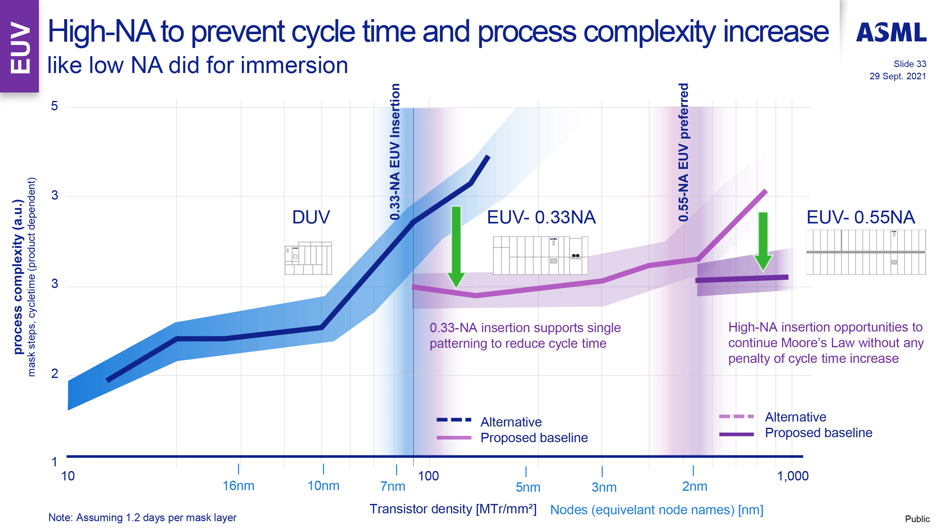
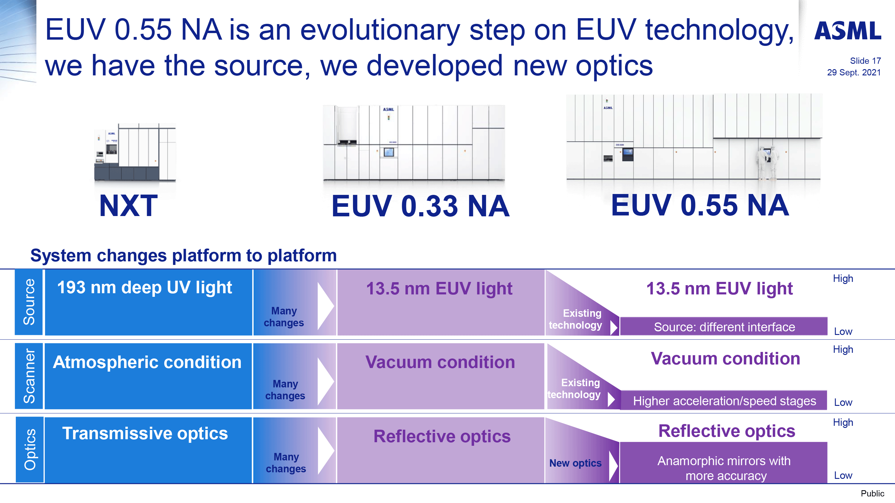
But ASML's Twinscan EXE lithography tools with a 0.55 NA will be significantly different than the company's regular Twinscan NXE litho machines with a 0.33 NA. An avid reader will remember from our previous reports that High-NA scanners are going to be significantly bigger than contemporary EUV scanners, which will require new fab structures. But these is by far not the only difference.
Perhaps the biggest change between the High-NA and regular EUV scanners is the halved reticle size of the High-NA scanners, which will require chipmakers to rethink how they design and produce chips – especially at a time when high-end GPUs and AI accelerators are pushing the limits for reticle sizes. In addition, since High-NA scanners will support a higher resolution and different reticle size, they will require new photoresists, metrology, pellicle materials, masks, and inspection tools, just to name some of the alterations. In short, High-NA tools will require significant investments in infrastructure to go with them.
Although semiconductor production infrastructure is developed by the whole industry, the best way to adopt it for real-world production is to tailor it for actual process technologies and process recipes. Which is why it is so important to start working with pilot scanners early to prepare for HVM using production machines.
Intel was the first company to order ASML's pilot Twinscan EXE:5000 scanner back in 2018. It was also the first to place an order for ASML's commercial grade Twinscan EXE:5200 litho tool in 2022. The company is set to start development work on its 18A node (18 angstroms, 1.8nm) in 2024 and then will employ High-NA tools for a post-18A node, presumably in 2025 – 2026.
By getting High-NA tools earlier than its rivals, Intel not only be able to ensure that its tools produce desired results, but it has a chance to set the standards for the industry when it comes to High-NA manufacturing. For Intel this might mean getting a significant advantage over its rivals, Samsung Foundry and TSMC.
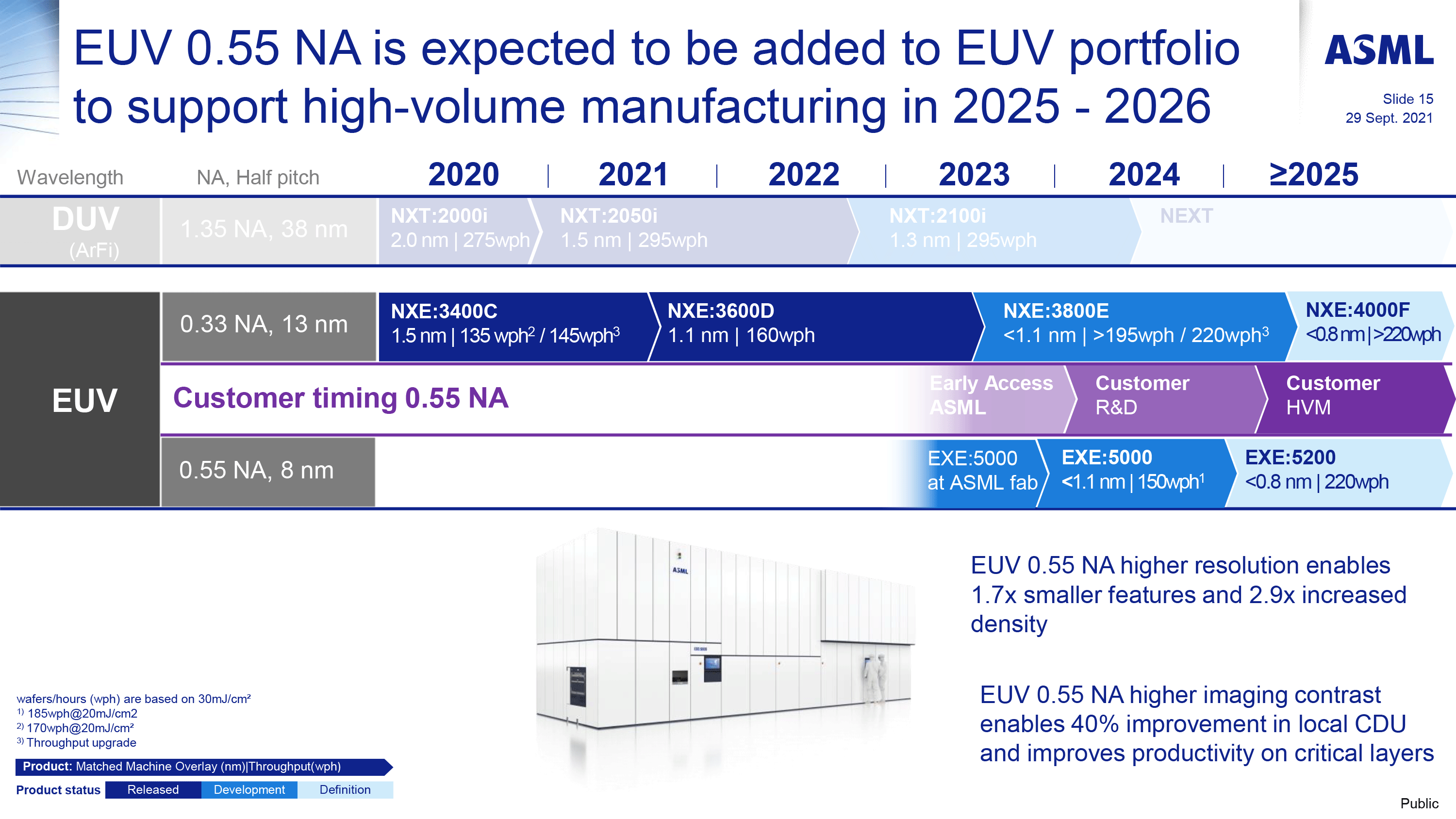
ASML announced in 2022 that it will be able to produce 20 High-NA EUV litho tools per year in 2027 - 2028. Meanwhile, the company disclosed earlier this year is that it had a double-digit number of machines in its High-NA backlog, which signals that its partners are set to adopt these scanners in the coming years. And leading that pack will be Intel.
Source: ASML (X)


28 Comments
View All Comments
PeachNCream - Thursday, December 21, 2023 - link
I hope that the arm injury heals well and the sling is no longer needed soon.wrkingclass_hero - Tuesday, January 2, 2024 - link
It's okay, he has 3 armsPeachNCream - Friday, January 5, 2024 - link
That would be annoying for someone living in the US. Imagine paying medical bills associated with one extra limb in with their disaster of a health care system.charlesg - Friday, January 5, 2024 - link
While funny, the "health care system" is doing precisely what it's designed to do: make massive amounts of money.It has little to do with "health", and hasn't for a very long time.
Oxford Guy - Friday, January 12, 2024 - link
DeSantis wants to raid Canada for its more-affordable prescription drugs.The connection to tech in this comment is extremely tenuous.
Back to the topic... people were musing about future transistor tech. I have been waiting for some sort of gallium arsenide since the Cray III. How about creating a machine that can build transistors from such a molecule — molecule by molecule? This will remove all of the defects and maximize the density. There has been talk about nanowires but it all seems very messy.
dontlistentome - Friday, December 22, 2023 - link
Wonder if they told the driver how much is load was worth?Threska - Saturday, December 23, 2023 - link
The other twelve were needed plus the crates. Three stories tall is about the size of a medium hydraulic press.Samus - Tuesday, January 9, 2024 - link
Seriously. The only thing more nerve-racking would be transporting an atomic bomb.rybba - Thursday, January 11, 2024 - link
Regarding nerve-racking transports you should watch Sorcerer (1977):nudge> - Friday, December 22, 2023 - link
It aint what you do, it's the way that you do it. That's what gets results...