Intel Xeon Sapphire Rapids: How To Go Monolithic with Tiles
by Dr. Ian Cutress on August 31, 2021 10:00 AM ESTAdd In Some HBM, Optane
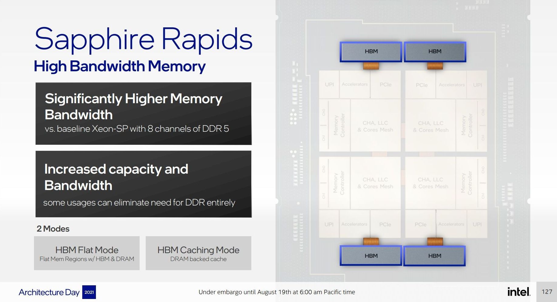
The other angle to Sapphire Rapids is the versions with HBM on board. Intel announced this back in June, but there haven’t been many details. As part of Architecture Day, Intel stated that that HBM versions of Sapphire Rapids would be made public, and be made socket compatible with standard Sapphire Rapids. The first customer of the HBM versions of SPR is the Argonne National Lab, as part of its Aurora Exascale supercomputer.
This diagram it showcases four HBM connections, one to each compute tile. Looking at the package, however, I don’t think that there’s realistically enough space unless Intel has commissioned some novel HBM that is long and narrow as it is in the diagram.
Even though Intel said that the HBM variants would be in the same socket, even their own slide from Hot Chips says different.
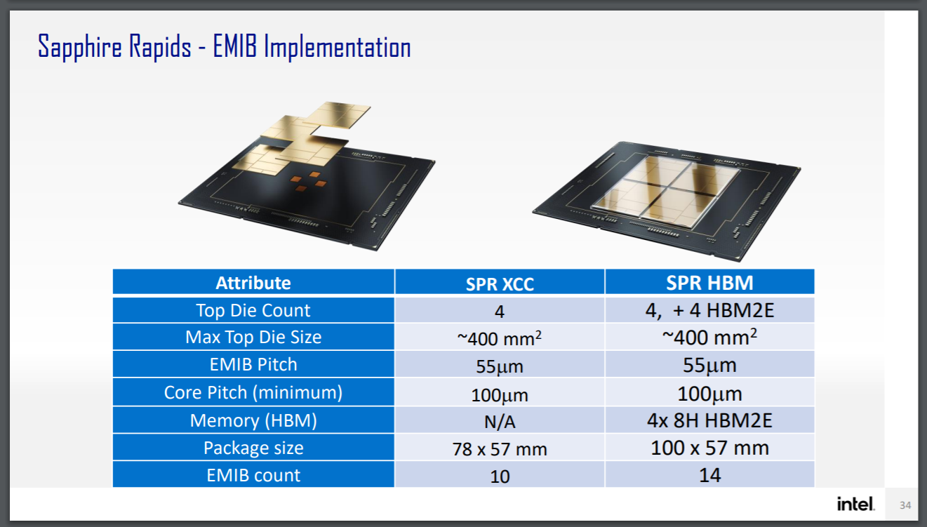
Here the package size with HBM says 100x57mm, compared to the SPR which is 78x57mm. So unless Intel is planning a reduced version for the 78x57mm socket, it's going to be in a different socket.
It is important to note that HBM will act in a similar capacity to Optane – either as an HBM flat mode with DRAM that equates the two, or as an HBM caching mode that acts similar to an L4 cache before hitting main memory. Optane on top of this can also be in a flat mode, a caching mode, or as a separate storage volume.
HBM will add power consumption to the package, which means we’re unlikely to see the best CPU frequencies paired with HBM if it is up against the socket limit. Intel has not announced how many HBM stacks or what capacities will be used in SPR, however it has said that they will be underneath the heatspreader. If Intel are going for a non-standard HBM size, then it’s anyone’s guess what the capacity is. But we do know that it will be connected to the tiles via EMIB.
A side note on Optane DC Persistent Memory – Sapphire Rapids will support a new 300 series Optane design. We asked Intel if this was the 200-series but using a DDR5 controller, and were told that no, this is actually a new design. More details to follow.
UPI Links
Each Sapphire Rapids Processor will have up to four x24 UPI 2.0 links to connect to other processors in a multi-socket design. With SPR, Intel is aiming for up to eight socket platforms, and in order to increase bandwidth has upgraded from three links in ICL to four (CLX had 2x3, technically), and moved to a UPI 2.0 design. Intel would not expand more on what this means, however they will have a new eight-socket UPI topology.
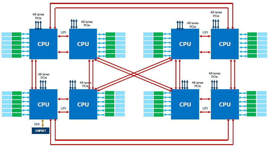
Current Intel Hypercube
Current eight-socket designs use a twisted hypercube topology: two groups of four form a box, and one pair is connected to the same vertex on the other set of four, while the second pair is inverted. Make sense? No, not really. Essentially each CPU is directly connected to three others, and the other four are two hops away. With the new topology, each CPU gets a direct connection to another, which moves the design more towards a fully connected topology, however exactly which CPU that connection should go to, Intel hasn’t stated yet.
Security
Intel has stated that it will be announcing full Security updates for SPR at a later time, however features like MKTME and SGX are key priorities.
Conclusions
For me, the improved cores, upgraded PCIe/DDR, and the ‘appears as a monolith’ approach are the highlights to date. However, there are some very obvious questions still to be answered – core counts, power consumption, how lower core counts would work (even suggestions that the LCC version is actually monolithic), and what the HBM enabled versions will look like. The HBM versions, with the added EMIB, are going to cost a good amount, which isn’t great at a time when AMD’s pricing structure is very competitive.
It is expected that when Sapphire Rapids is released, AMD will still be in the market with Milan (or as some are postulating, 3D V-Cache versions of Milan, but nothing is confirmed) and it won’t be until the end of 2022 when AMD launches Zen 4. If Intel can execute and bring SPR into the market, it will have a small time advantage in which to woo potential customers. Ice Lake is being sold on its specific accelerator advantages, rather than raw core performance, and we will have to wait and see if Sapphire Rapids can bring more to the table.
Intel moving to a tile/chiplet strategy in the enterprise has been expected for a number of years – at least on this side of the fence, ever since AMD made it work and scale beyond standard silicon limits, regardless of whatever horse-based binding agent is used between the silicon, Intel would have to go down this route. It has been delayed, mostly due to manufacturing but also optimizing things like EMIB which also takes time. EMIB as a technology is really impressive, but the more chips and bridges you put together, even if you have a 99% success rate, that cuts into yield. But that's what Intel has been working on, and for the enterprise market, Sapphire Rapids is the first step.


94 Comments
View All Comments
Spunjji - Tuesday, August 31, 2021 - link
So...Lots of cores probably, but we don't know how many.
No word on costs, but 4 large dies on a process that has yet to yield well + EMIB with high-power chips + double the number of masks required for the product doesn't speak to being economical.
CXL 1.1, only not exactly, just bits of it.
Lots of AI-friendly stuff, but people are already doing AI stuff on dedicated accelerators.
Moar Sockits, though! Whee!
Honestly, I'm a little concerned. This looks like it's going to be wildly expensive and not very compelling. I hope the smaller dies are a little less absurd.
Kamen Rider Blade - Tuesday, August 31, 2021 - link
According to leaks, 14 Cores per Tile is the Max / (100%) yield.2 of the spots that would be used for a 4x4 2D-array of cores is used for Inter-connect management.
repoman27 - Tuesday, August 31, 2021 - link
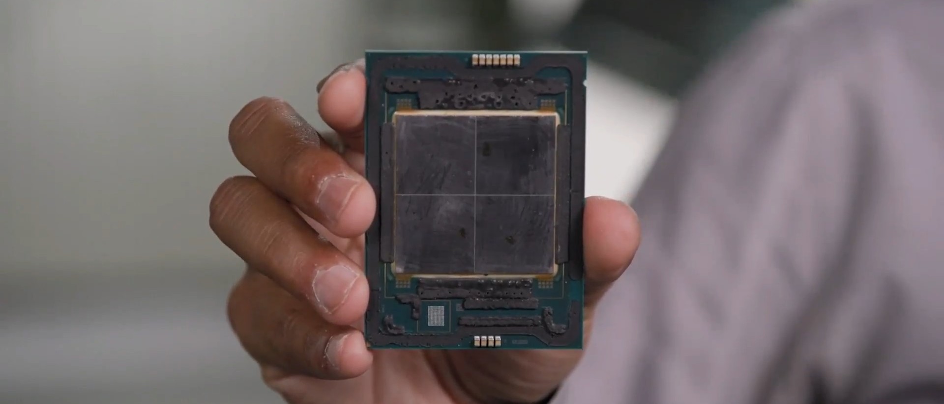
Someone has already disassembled and posted images of a Sapphire Rapids XCC engineering sample: https://www.bilibili.com/read/cv11692201 The SPR XCC SKUs are expected to top out at 56 cores, however, the individual dies clearly feature a 4x4 grid with 15 CPU core tiles plus an IMC tile (for the two DDR5 controllers). The dies are 426 mm², and according to the roadmaps at least one CPU core per die will be disabled.Intel typically produces three floorplan designs for each Xeon Scalable generation, e.g. XCC, HCC, and LCC. While they are burning two tape-outs with the left and right XCC dies for SPR, there is also supposedly an up to 34 core MCC product in the works. If Intel were to add another column to the XCC die—three more CPU core tiles and another IMC tile—they would end up with an 18-core die with four memory channels. A two die package would have up to 36 cores (or 34 with at least one core disabled on each die) and still have 8-channel memory. An 18-core, 4-channel HEDT or workstation product would also be possible using a single die.
Spunjji - Tuesday, September 7, 2021 - link
Interesting. That would certainly help to fill out a bunch of products further down the line, but wouldn't it also require double the masks to produce a mirror design of the die?Still, it (alongside the process improvements) should at least help end the yield problems they've had with Ice Lake SP.
WaltC - Tuesday, August 31, 2021 - link
I always get a kick these days to see "Intel's Process 7" stated with a straight face and no qualifier. Trying desperately to achieve some sort of marketing-level process equality with AMD/TSMC (who can unashamedly and accurately say "7nm".) This is what "we're behind" marketing looks like, I guess. Intel seems to have learned a lot from its previous association with Apple--well, at least in terms of marketing...;)WaltC - Tuesday, August 31, 2021 - link
Wanted to add that all of this wordage used to describe vaporware is beginning to remind me of a lot of Larrabee. Although to be fair, I really do think that at some point Intel will have something to sell here...at some point. That'll be nice because then we won't be discussing vaporware any longer.Wrs - Tuesday, August 31, 2021 - link
What if I tell you they're technically close to equivalent to TSMC 7 and Samsung 5? You can specify a process to be as advanced as you want, the question is whether/how well you can build it. Originally what was called Intel 10nm was very ambitious, way better than TSMC's 10nm. Only it would take Intel 7 years in between nodes rather than the expected 2-3, giving TSMC all the time to catch up and more. Today TSMC is in pole position - we're just waiting for their 5 to mature to reach desktop/server power density.Calin - Wednesday, September 1, 2021 - link
The "nanometers" you're so faithful to are just a small bit of the entire wafer-to-microprocessor saga. Intel, Global Foundries (ex-AMD), TSMC, Samsung and the others have different measurements in all of these areas, and some production choices are better than other.The "Feature Size" (the so-called nanometers) is not the only "measuring stick" - you also have vias (i.e. the width of the electrical connections), the uniformity with which you can produce something (leading to a lower voltage overall, as there are no "outliers" that need that extra voltage to work), ...
As for "transistor density" - this varies across processes and process variants, and is also affected by the "library" (high density or low density - one for the most transistors at lower power, the other with less transistors on the same area but it has better frequency and can cool a higher power-per-transistor).
Anyway, here's an article with helpful pictures - Intel 10nm is relatively similar to TSMC 7nm in density, it's below just by a bit and not by the 49% straight math would suggest (i.e. 10x10=100 transistors in a 70nmx70nm square for TSMC and 7x7=49 transistors for Intel 10nm).
https://hexus.net/tech/news/cpu/145645-intel-14nm-...
Foeketijn - Wednesday, September 1, 2021 - link
I agree, but like to add Intels 10nm is about as small as the TSMC 7nm. It's like, at what height do you measure the treetrunks width.drothgery - Wednesday, September 1, 2021 - link
Process names have been marketing, not measurements of any actual feature size since they were naming processes by microns. And others have noted that what Intel's calling Intel 7 now is pretty similar density to TSMC N7 for CPUs. I'd also note that TSMC's actual name for what's commonly called their "7nm" is "N7", not "7nm"; no nanometers there either.