Intel's Process Roadmap to 2025: with 4nm, 3nm, 20A and 18A?!
by Dr. Ian Cutress on July 26, 2021 5:00 PM ESTIntel’s Next Generation Packaging: EMIB and Foveros
Alongside the process node advancements, Intel also has to march forward with next-generation packaging technology. The demand for high performance silicon coupled with increasingly difficult process node development has created an environment where processors are no longer a single piece of silicon, relying on multiple smaller (and potentially optimized) chiplets or tiles to be packaged together in a way that benefits performance, power, and the end product.
Single large chips are no longer the smart business decision – they can end up too difficult to make without defects, or the technology to create them isn’t optimized for any one particular feature on the chip. However, dividing a processor up into separate silicon pieces creates additional barriers to moving data around between those pieces – if the data has to transition from being in silicon to being in something else (such as a package or an interposer) then there is a power cost and latency cost to consider. The tradeoff is optimized silicon built for purpose, such as a logic chip made on a logic process, a memory chip made on a memory process, and the smaller chips often have better voltage/frequency characteristics when binning than their larger counterparts. But underpinning all of this is how the chips are put together, and that requires packaging.
Intel’s two main specialist packaging technologies are EMIB and Foveros. Intel explained the future of both in relation to its future node development.
EMIB: Embedded Multi-Die Interconnect Bridge
Intel’s EMIB technology is designed for chip-to-chip connections when laid out on a 2D plane.
The easiest way for two chips on the same substrate to talk to each other is by taking a datapath through the substrate. The substrate is a printed circuit board made of layers of insulated material interspersed with metal layers etched into tracks and traces. Depending on the quality of the substrate, the physical protocol, and the standard being used, it costs a lot of power to transmit data through the substrate, and bandwidth is reduced. But, this is the cheapest option.
The alternative to a substrate is to put both chips onto an interposer. An interposer is a large piece of silicon, big enough for both chips to wholly fit on to, and the chips are bonded directly to the interposer. Similarly there are data paths put into the interposer, but because the data is being moved from silicon to silicon, the loss of power is not as much as a substrate, and the bandwidth can be higher. The downside to this is that the interposer also has to be manufactured (usually on 65nm), the chips involved have to be small enough to fit, and it can be rather expensive. But, the interposer is a good solution, and active interposers (with built in logic for networking) have yet to be fully exploited).
Intel’s EMIB solution is a combination of both interposer and substrate. Rather than taking a large interposer, Intel uses a small slither of silicon and embeds that directly into the substrate, and Intel calls this a bridge. The bridge is effectively two halves with hundreds or thousands of connections each side, and the chips are built to connect to one half of the bridge. Now both chips are connected to that bridge, having the benefit of transferring data through silicon without the restrictions that a large interposer might bring. Intel can embed multiple bridges between two chips if more bandwidth is needed, or multiple bridges for designs using more than two chips. Also, the cost of that bridge is much less than a large interposer.
First Generation EMIB
With those explanations, it sounds like Intel’s EMIB is a win-win. There have been a few limitations to the technology – actually embedding a bridge into a substrate is kind of hard. Intel has spent several years and lots of money trying to perfect the technology for low power operation. On top of this, whenever you are adding multiple elements together, there is an associated yield with that process – even if connecting a chip to a bridge has a 99% yield, doing it with a dozen chips on a single design reduces the overall yield down to 87%, even when starting with known good chips (that have their own yield). When you hear that Intel has been working on bringing this technology to volume, it is these numbers they are trying to improve.
Intel currently has EMIB in the market on several of its products, most noticeably its Stratix FPGA and Agilex FPGA families, but it was also part of its Kaby G line of mobile processors, connecting a Radeon GPU to high-bandwidth memory. Intel has already stated that it is coming to several future products, such as Ponte Vecchio (supercomputer-class graphics), Sapphire Rapids (next generation Xeon enterprise processor), Meteor Lake (2023 consumer processor), and others related to graphics.

Intel's Ponte Vecchio uses EMIB and Foveros
On the roadmap side of EMIB, Intel is reducing the bump pitch over the next few years. When the chips are connected to the bridges embedded in the substrate, they connect across bumps, and the distance between the bumps is known as the pitch – the smaller the bump pitch, the more connections can be made in the same area. This allows the chip to either increase bandwidth, or reduce the bridge size. The first generation EMIB technologies in 2017 were using 55 micron bump pitches, and that still appears to be the case with upcoming Sapphire Rapids (see my comment about the time it has taken Intel to get it right), however Intel is aligning itself with a 45 micron EMIB beyond Sapphire Rapids, leading to a 36 micron EMIB in its third generation. The timescales for these were not disclosed, however post Sapphire Rapids would be Granite Rapids, so that might be where the 45 micron design comes to market.
Foveros: Die to Die Stacking
Intel introduced its die-to-die stacking technology in 2019 with Lakefield, a mobile processor designed for low idle power designs. That processor has since been put on End of Life proceedings, but the idea is still integral to the future of Intel’s future product portfolio and foundry offerings.
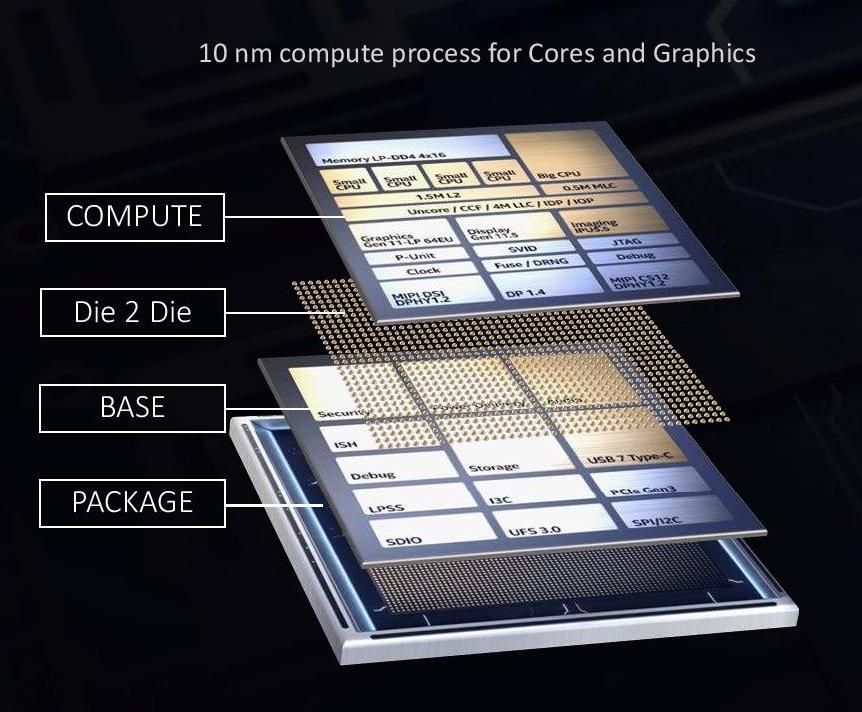
Intel’s die-to-die stacking is to a large extent very similar to the interposer technology mentioned in the EMIB section. We have one piece of silicon (or more) on top of another. In this instance however, the interposer, or base die, has active circuitry relevant for the full operation of the main compute processors found in the top piece of silicon. While the cores and graphics were on the top die in Lakefield, built on Intel’s 10nm process node, the base die had all the PCIe lanes, USB ports, security, and everything low power related to IO, and was built on a 22FFL low power process node.

So while EMIB technology splitting the silicon to work alongside each other is known as 2D scaling, by placing the silicon on top of each other we have entered a full 3D stacking regime. This comes with some good benefits, especially at scale – data paths are a lot shorter, leading to less power loss due to shorter wires but also better latency. The die-to-die connections are still bonded connections, with the first generation at a 50 micron pitch.
But there are two key limitations here: thermals and power. To avoid problems with thermals, Intel made the base die have very little logic and used a low power process. With power, the issue is enabling the top compute die to have power for its logic – this involves large power through-silicon-vias (TSVs) from the package up through the base die into the top die, and those TSVs carrying power become an issue for localized data signaling due to interference caused by high currents. There is also a desire to scale to smaller bump pitches in future processes, allowing for higher bandwidth connections, requiring more attention to be paid by the power delivery.
The first announcement related to Foveros today is regarding a second generation product. Intel’s 2023 consumer processor, Meteor Lake, has already been described above as using an Intel 4nm compute tile, taking advantage of EUV. Intel is also stating today that it will be using its second generation Foveros technology on the platform, implementing a bump pitch of 36 micron, effectively doubling the connection density over the first generation. The other tile in Meteor Lake has not been disclosed yet (either what it has or what node it is on), however Intel is also stating that Meteor Lake will scale from 5 W to 125 W.
Foveros Omni: Third Generation Foveros
For those that have been following Intel’s packaging technologies closely, then the name ‘ODI’ might be familiar. It stands for Omni-Directional Interconnect, and it was the moniker being floated in previous Intel roadmaps regarding a packaging technology that allows for cantilevered silicon. That is now going to be marketed as Foveros Omni.
This means that the limit of the first generation Foveros which needed a top die smaller than the base die is now removed. The top die can be larger than the base die, or if there are multiple die on each of the levels, they can be connected to any number of other silicon. The goal of Foveros Omni is really to solve the power problem as discussed in the initial section on Foveros – because power carrying TSVs cause a lot of localized interference in signaling, the ideal place to put them would be on the outside of the base die. Foveros Omni is a technology that allows for the top die to overhang from the base die and copper pillars are built from the substrate up to the top die to provide power.
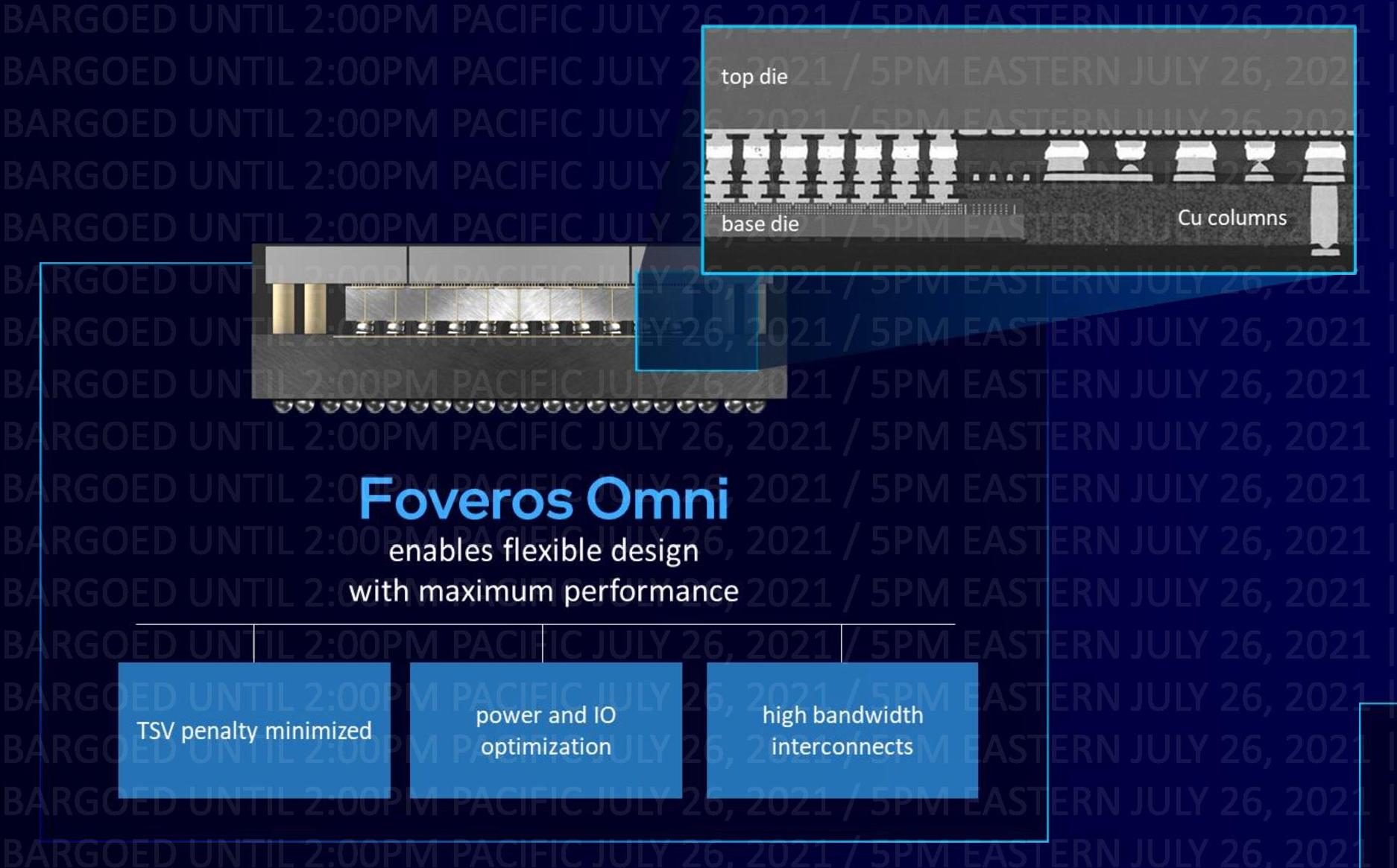
With this technology, if power can be brought in from the edges of the top die, then this method can be used. I did wonder, however, that with large silicon if power would be better fed right up the middle – Intel has stated that Foveros Omni works with split base dies, such that power carrying copper pillars could be placed in the middle of the design if the base die is designed for substrate to be available on that lower layer.
By moving the power TSVs outside the base die, this also allows for a die-to-die bump pitch improvement. Intel is citing 25 microns for Omni, which would be another 50% increase in bump density over second generation Foveros. Intel is expecting Foveros Omni to be ready for volume manufacturing in 2023.
Foveros Direct: Fourth Generation Foveros
One of the issues with any die-to-die connectivity is the connection itself. In all of these technologies mentioned so far, we’re dealing with microbump bonded connections – small copper pillars with a tin solder cap, which are put together and ‘bonded’ to create the connection. As these technologies are growing copper and the depositing tin solder, it gets difficult to scale them down, plus there is also the power loss of the electronics transferring into the different metals. Foveros Direct gets around this problem, by doing direct copper-to-copper bonding.
Rather than rely on pillars and bumps coming together, the concept of direct silicon-to-silicon connectivity has been researched for a number of years. If one piece of silicon is lined up directly with another, then there is little-to-no need for extra steps to grow copper pillars and such. The issue comes with making sure that all the connections are made, ensuring that both the top die and bottom die are so incredibly flat that nothing can get in the way. Also, the two pieces of silicon have to become one, and are permanently bonded together without any way of coming apart.
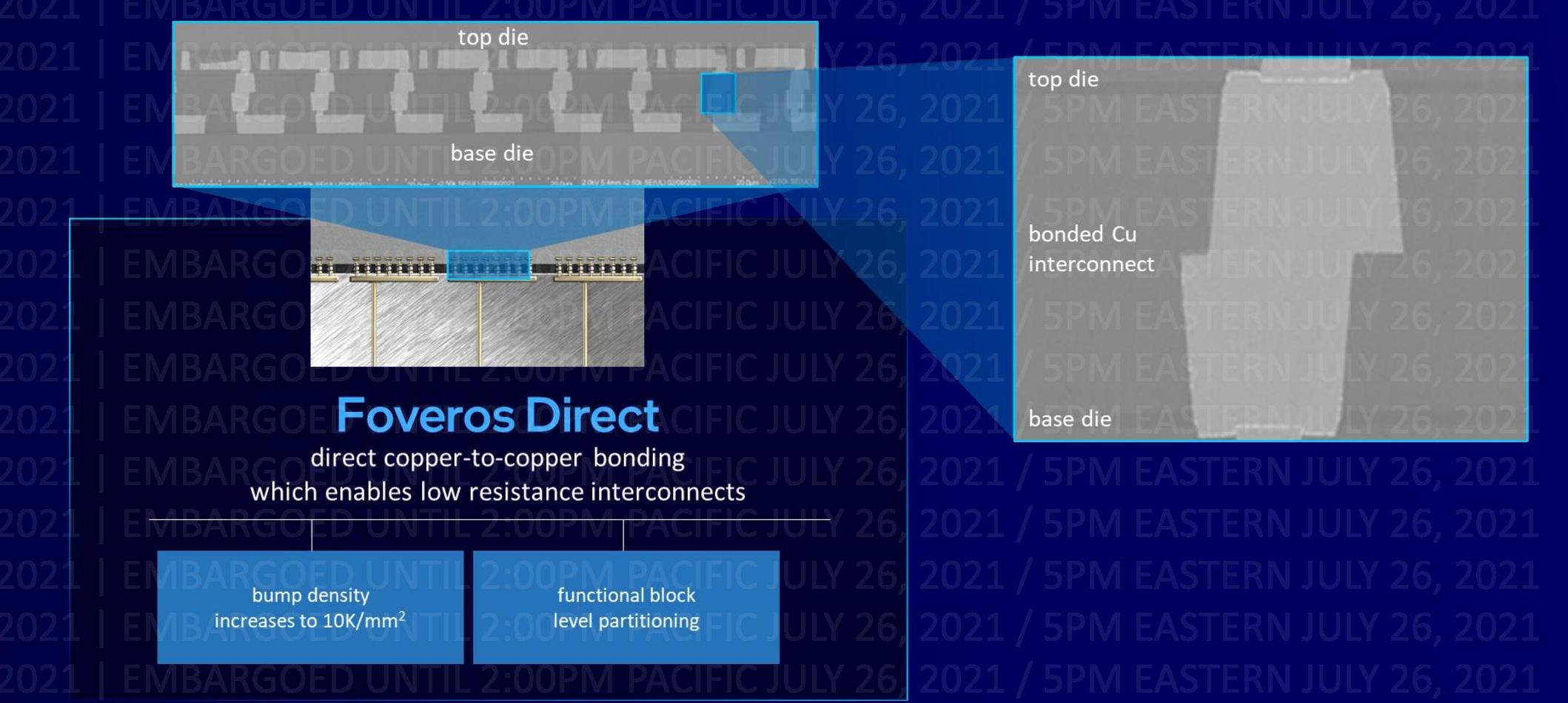
Foveros Direct is a technology that helps Intel drive the bump pitch of its die-to-die connections down to 10 micron, a 6x increase in density over Foveros Omni. By enabling flat copper-to-copper connections, bump density is increased, and the use of an all-copper connection means a low resistance connection and power consumption is reduced. Intel has suggested that with Direct, functional die partitioning also becomes easier, and functional blocks could be split across multiple levels as needed.
Technically Foveros Direct as a die-to-die bonding could be considered complimentary to Foveros Omni with the power connections outside the base die – both could be used independently of each other. Direct bonding would make internal power connections easier, but there would still be the issue of interference perhaps, which Omni would take care of.
It should be noted that TSMC has a similar technology, known as Chip-on-Wafer (or Wafer-on-Wafer), with customer products set to come to the market in the coming months using 2-high stacks. TSMC has demonstrated a 12-high stack in mid-2020, however this was a test vehicle for signaling, rather than a product. The issue going up in stacks is still going to be thermals, and what goes into each layer.
Intel predicts that Foveros Direct, like Omni, will be ready for mass volume in 2023.


326 Comments
View All Comments
Oxford Guy - Wednesday, August 11, 2021 - link
Says the person who said, in reply to one of my posts ‘we know you’re smart ... use your powers for good’.You typically post whatever sounds reasonable at a given time, no matter how inaccurate it is. I, by contrast, am capable of remembering what has been said — the positions that have been taken.
One cannot simultaneously claim I’m obviously intelligent and that my posts are valid. One cannot also post ‘agreed’ — as you did in another topic whilst pretending that my posts are vapid — unless you’re with that very vapidity.
I also find it droll that you employ the royal ‘we’ here. Are you a member of staff or merely that entitled?
Oxford Guy - Wednesday, August 11, 2021 - link
And... please — for the benefit of this forum...Learn the list of common logical fallacies. Your latest use of ad baculum is only worthy of yet another eyeroll.
mode_13h - Thursday, August 12, 2021 - link
> Says the person who said, in reply to one of my posts ‘we know you’re smart> ... use your powers for good’.
There's no logical inconsistency, there. Most of your posts seem to pull threads off-topic and offer little of value to the original subject. And quite a few are just snarky, cynical trolls.
> You typically post whatever sounds reasonable at a given time
I try to engage my brain and look at the other side of an issue, or at least from a perspective other than my narrow self-interest. And most often, what draws me to the other side of an issue is when someone takes an extreme position or makes absolutist statements that seem unjustified. If there's one thing you could say I consistently oppose, it's oversimplification.
> no matter how inaccurate it is.
Ah, now that's interesting. Accuracy is rooted in fact. And the facts are where you completely fall apart. You consistently fail to support your claims and assertions with good & relevant sources.
With that said, if I post something that's demonstrably inaccurate, then please do us *all* a favor and point it out. I never claimed to know everything or be infallible. I've even learned things from debates and spirited discussions.
> I, by contrast, am capable of remembering what has been said —
> the positions that have been taken.
This might blow your mind, but I have actually changed positions, on a few occasions. Not many, but I'm actually willing to re-evaluate my position, after looking at the arguments on both sides.
Also, I try not to be overly partisan, which is to say that I try not to take a side of an issue purely on the basis of political allegiance or preoccupation with self-consistency. If I think one side is overstating their case or otherwise acting in bad faith, I might come out against their position, even while I might've previously been supportive on another issue.
> One cannot simultaneously claim I’m obviously intelligent and that my posts are valid.
Why not? Intelligence describes the actor, while the writing of posts describes their actions. I can criticize the latter, without invalidating the former. Plenty of smart people do things that are thoughtless, counterproductive, antisocial, or worse. However, at some point, the actions do begin to define the actor.
> One cannot also post ‘agreed’ — as you did in another topic whilst pretending
> that my posts are vapid
I said they're "consistently", not "uniformly" or "without exception". If I thought you were a complete waste of time, then I wouldn't spend so much time replying to you.
> unless you’re with that very vapidity.
Well, I'm not going to claim I've never made a vapid post. I try to say things worth saying, but I'm not infallible. It is just a news comment thread, and I don't worry too much about a post here or there.
> I also find it droll that you employ the royal ‘we’ here.
It wasn't. I was speaking on behalf of myself AND other forum participants. That it was preceded by "I think", signifies it as a speculative statement. Others are welcome to disagree.
ikjadoon - Monday, July 26, 2021 - link
What? Intel has long sandbagged its numbers. Unfortunately, we've all decided to follow the marketing, so yeah, at least Intel is more honest now. But none of it matters until they deliver it. I'm not trusting any marketing announcements from Intel. I want the desktop / laptop CPU in-hand so that there's actual benchmarks.//
https://www.tsmc.com/english/dedicatedFoundry/tech...
Otherwise there's no need for the TSMC marketing dept to magically shrink the fake 16nm node to become a fake 12nm.
>An enhanced version of TSMC's 16nm process was introduced in late 2016 called "12nm".
https://en.wikichip.org/wiki/16_nm_lithography_pro...
mode_13h - Monday, July 26, 2021 - link
> at least Intel is more honest now.Wow, that sure takes some mental gymnastics to see Intel participating in the same disinformation race as "more honest".
You could say they're being more consistent... until TSMC and Samsung decide to rebrand their process nodes to stay ahead of Intel's naming.
All of this argues that it's an exercise in futility to pretend these names actually mean anything. They should just use codenames, or maybe a completely arbitrary schema involving sequential numbering + letters or Greek alphabet characters.
ikjadoon - Tuesday, July 27, 2021 - link
Sure, noted. "More honest" relative to the industry = more consistent. I'm flabbergasted how anyone has any problem with this, when literally no one had a problem TSMC & Samsung have done this for years, lol.OK? Why wouldn't TSMC & Samsung play more bullshit w/ foundry marketing? They started it a while ago, so it's more than expected to continue. Good technology has never needed exaggerations: Intel, TSMC, and Samsung all know that.
lol, this is just the tip of the iceberg of marketing. We don't need "i7" or "Ryzen 3", either. How deep do you want to go?
Node names *absolutely* mean something: it's the progression within a foundry. Almost nobody dual-sources CPUs any more, but everyone wants to play "Fantasy Nodes".
That's the more interesting problem. Why is the peak density leap between 10->7 larger than 7->4? Because, clearly, density is not the *only* metric involved in a node.
mode_13h - Wednesday, July 28, 2021 - link
> literally no one had a problem TSMC & Samsung have done this for years, lol.How do you know? Did you run a survey?
Unlike what Intel is doing, Samsung and TSMC never had a press conference to announce they're going to use more dishonest naming. If they had, you'd probably have seen the same kind of sentiment you're seeing when Intel did just that.
> Good technology has never needed exaggerations
That's not true. Not as long as exaggerations can help you sell a little more. Nvidia exgerates like all damn day, even while they've been sitting comfortably atop the heap.
> it's the progression within a foundry
Right, so the names just need to reflect that. Like I said, they should use sequential numbering for big steps, and then letter suffixes to denote minor iterations.
> density is not the *only* metric involved in a node.
All the more reason to cut ties between their naming and any pretense of density.
wut - Thursday, July 29, 2021 - link
"Right, so the names just need to reflect that. Like I said, they should use sequential numbering for big steps, and then letter suffixes to denote minor iterations"Tell TSMC, Samsung, along with everyone else to do it, at the same time.
(TSMC with its N7+, N5P, and Samsung with its 3GAE...)
If you want to apply some standard, apply it to everyone first. Lest you'd be the one who ends up looking agenda-ladened.
mode_13h - Sunday, August 1, 2021 - link
> Tell TSMC, Samsung, along with everyone else to do it, at the same time.The beauty of it is that Intel can simply opt out of the game, without requiring others to do the same.
> If you want to apply some standard
No, you don't have to replace a false standard with another standard (false or not). The point is just to drop the pretense that the node names really mean anything.
twtech - Tuesday, July 27, 2021 - link
A really bold move would have been to move away from "nm" naming altogether and call it 100D or something for 100 million transistor density.