The Intel Lakefield Deep Dive: Everything To Know About the First x86 Hybrid CPU
by Dr. Ian Cutress on July 2, 2020 9:00 AM ESTThe Future of Lakefield
Lakefield as a product is a lateral move for Intel. The company is taking some of its new and popular IP, and placing it into a novel form factor that has required a significant amount of R&D from a manufacturing and construction perspective. The goal of Lakefield was to meet particular customer requirements, which we understand to be around battery life, performance, and multi-screen support, and according to Intel, those goals have been met, and they will be producing future generations of Lakefield products.
In particular, Intel has produced this slide at a couple of conferences.
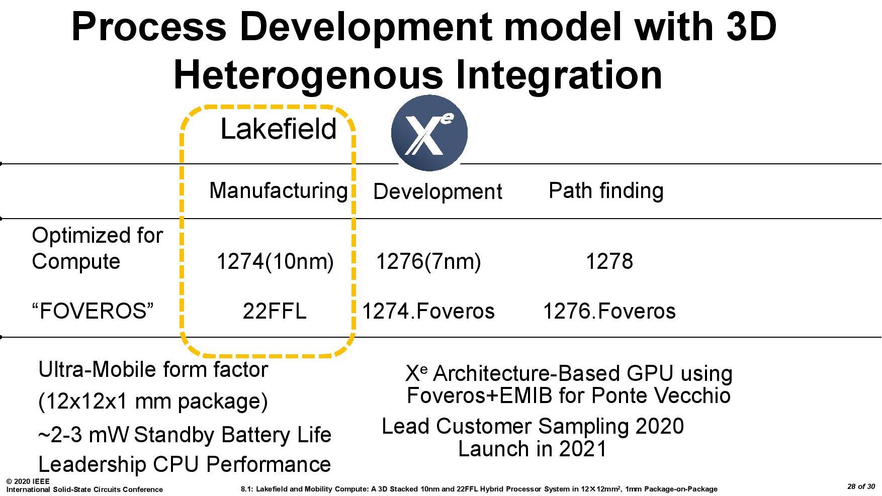
This slide essentially states that Lakefield product in the yellow box has two silicon die – one optimized for compute on Intel’s P1274 process (10+ nm) and the Foveros layer (the active interposer layer) on Intel’s 22FFL process.
The next product with heterogeneous manufacturing integration will be Intel’s big Xe-HPC product, Ponte Vecchio, which will use Intel’s P1276 process (7nm) as a compute die and Intel’s P1274 (10+) process as a base interposer layer.
Beyond this, Intel looks to continue with its multi-layered products by having the compute layer on the most advanced process node, with the interposer layer one generation behind, on a ‘Foveros’ optimized variant.
So the first generation Lakefield is essentially a product that combines P1274 and 22FFL, and a future product is likely to be built on P1276 on the compute layer and P1274 for the interposer layer. Keeping this sort of cadence makes a lot of sense. However, Intel is going to have to learn from Lakefield in a number of ways, especially as we look at ways in which the heterogeneous layering concept can expand. I’ve split this into several areas that I feel is critical to where layered processors can really make a difference.
Growing a Stacked Die to Higher TDP and Core Count
I’ve combined these two points because they essentially go together. Implementing two simple silicon die together in a small form factor product, while is interesting on the power side of the equation, doesn’t probe the question of scaling the product up. It’s easy enough to scale the product out by adding in some form of connectivity to the stack and then connecting them together (which is what’s happening in Ponte Vecchio), but at some point the stack has to move to a higher level of power consumption if it wants to move upwards in power.
This means that thermals become a bigger issue if it wasn’t already. If we take the current Lakefield design, with one compute die over an active interposer, with the right routing then moving to a physically larger floorplan and a higher power shouldn’t be too much of an issue – if anything, making the base die larger should help spread a lot of that IO about, making the interposer a functionally less active interposer. Or Intel will implement the next generation of its die-to-die stacking technology, where the top dies can be larger than the base dies, in a cantilevered fashion.
The bigger deal with the thermals is going to be on the top, with the stacked PoP memory. We go more into the memory communications aspect in a bit, but ideally that memory needs to be on the side so the compute die can have access to a proper heatspreader. The only reason it is stacked in Lakefield is because of the size constraints and attempting to get everything into that small form factor. For anything larger, there needs to be a memory controller that looks outside the chip, which is kind of what we’re expecting from Ponte Vecchio with HBM. A desktop-class product would likely be in the middle.
Growing a Stacked Die to More Stacks
The other angle for a stacked silicon product is to put more stacks in place. This again brings about the question on cooling between the stacks, depending on what is actually there. Lakefield is only two stacks right now, with one high-powered stack and one low-powered stack. Intel would have to prove that it could manage multiple high-powered stacks in order to expand compute in the vertical dimension, but that brings about its own problems.
To start, with Lakefield, the main power to the top compute die is provided with TSVs going through the active interposer layer. For each compute die in a multi-die stack, there would have to be TSVs for each one in order to provide individual power. Unless the active interposer also acted as a PMIC, this could become difficult depending on what other TSVs or data paths need to be put in place between the layers.
Note, when we spoke with Intel’s Ramune Nagisetty at IEDM last year, when asked if Intel would ever discuss if a stacked product would use ‘dummy’ layers to help in cooling, we were told that this would unlikely be mentioned, focusing only on the layers that actually do any work. But ultimately there could be cause for dummy layers to aid in cooling, such that they can provide mass and distance between thermal hotspots between compute dies involved. As the number of layers increases, however, something like Lakefield would have to move the PoP memory off the top, as already mentioned.
Memory Communications
One element to the Lakefield design we haven’t really covered here is how the memory communicates. In the current Lakefield design, the compute cores and the memory controllers are located on the compute die. In order for a portion of main memory to be read into the compute die, the communication has to travel down through the active interposer, go into the package, and then loop back up to the stacked memory.
In the following diagram, on the left, we have (1) going from Compute Die to DRAM, and (2) DRAM back to Compute Die.
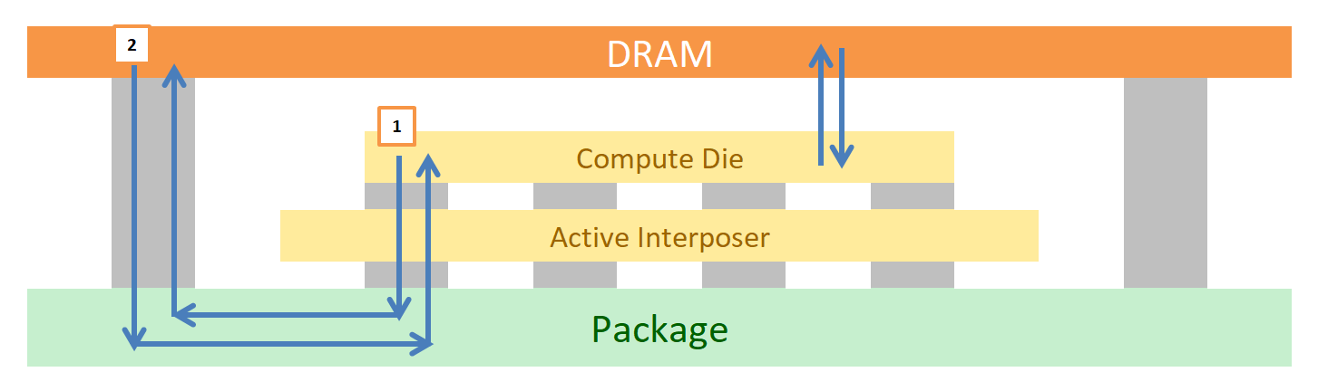
This path is a lot longer than simply going from the compute die straight up into the memory, which would be theoretical on the right hand side if the two were bonded and had appropriate pathways.
If a future Lakefield product wants to continue down the memory-on-top route, one optimization could be to bond that top memory die in a Foveros-like fashion. One could argue that it means Intel would have to bond the memory on at the manufacturing stage, but this already happens with the current generation of Lakefield designs. The only downside would be getting the bonding pads on the top of the compute die and the bottom of the memory die to line up, and then manage the communications from there. The power for the memory would have to also come through on TSVs.
But if we’re bonding the memory into the stack, then technically it could go at any layer – there are likely benefits to keeping the compute die/dies on top. This could lead to multiple layers of memory as needed.
Power Management
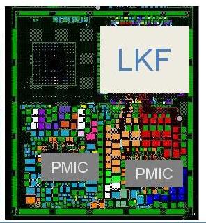
With the current Lakefield design, both the compute die and the active interposer die have their own power management IC (PMICs) in order to help deliver power. Based on Intel’s own diagrams, these PMIC designs take up more physical PCB space than Lakefield itself.
At some level, Intel is going to have to figure out to create a unified PMIC solution to cover every layer on the product. It likely reduces board space and would make things a lot simpler, as it does with laptops that can manage power to the CPU and GPU on the same die with an onboard power controller. A PMIC that can scale with layer counts is obviously going to be a plus.
Cooling
Through all of this, as I’ve mentioned several times, cooling is going to be a major concern. There’s no easy way around the physics of dissipating 5-10 W in such a small space, or over 100 W if the product scales up into something in a form factor that has a wider appeal. Previously in the article I mentioned that we had discussed this with Intel, and how areas such as microfluidic channels have obviously had some research put into, but nothing to the point where it could be done commercially and at scale. It’s a paradigm worth solving, because the benefits would be tremendous.
Beyond Windows and Enabling 5G
One thing to note is that Intel's Lakefield is only planned with Windows 10 support right now. Linux is currently not in the plan for this product, but it would have to be if Intel wants wider adoption of the technology.
Not only this, but as most people are comparing these devices to Qualcomm's hardware, appropriate 5G support will need to be applied - the current generation Lakefield is not part of Intel and Mediatek's collaboration on 5G, which only applies to Tiger Lake and beyond. Lakefield customers will have to rely on 4G as an optional extra, or 5G through an external modem.
The Future Of Lakefield
Even if this first generation version of Lakefield gets slammed pretty hard in performance-focused benchmark reviews for being slower than a dual-core Whiskey Lake, Lakefield marks some very big steps for Intel. Hybrid CPU designs, and stacked die-to-die connectivity, are going to feature in Intel’s future roadmaps – at what points will depend on how much Intel is willing to experiment but also how well Intel can execute. There have been discussions on Intel perhaps looking at an 8+8 hybrid CPU design in the future, although nothing we can substantiate, but we do know that Ponte Vecchio with stacked die is coming in late 2021.
One of the key ingredients in all of this is going to be at what points Intel’s technology portfolio is going to intersect its product portfolio. Some of these technologies might find their way better suited to aspects such as 5G networking, or automotive, rather than something we can consume on the desktop. As far as Lakefield goes, this first generation is going to be a rough challenge for Intel – they are pitching a low performance product in a high-cost segment based on technology (and to a certain extent, battery life). Die-to-die stacking will get easier to do as scale ramps, and hopefully new process node technologies will drive the power efficiency of those big cores lower to enable 2+4 or bigger designs when in a stacked form factor.
We eagerly await a chance to test 1st Gen Lakefield, but we’re also keeping an eye on what might be in the second and third generations.


221 Comments
View All Comments
returnzer0 - Friday, July 3, 2020 - link
So no, they did not, in fact, read the same article.s.yu - Monday, July 6, 2020 - link
Mystery solved!vanilla_gorilla - Friday, July 3, 2020 - link
https://www.anandtech.com/show/15877/intel-hybrid-..."At the top is the single Sunny Cove core, also present in Ice Lake. Intel has stated that it has physically removed the AVX-512 part of the silicon, however we can still see it in the die shot. This is despite the fact that it can’t be used in this design due to one of the main limitations of a hybrid CPU. We’ll cover that more in a later topic."
It was NOT physically removed but it cannot be used so it doesn't really matter. In practice this will have no AVX-512.
dotjaz - Friday, July 3, 2020 - link
Also "However, all modern software assumes a homogeneous processor", that's why they have to support exactly the same ISA extensions. I didn't realise Windows is the only modern software in existence.Meteor2 - Friday, July 3, 2020 - link
Why so rude, dotjaz?dotjaz - Saturday, July 4, 2020 - link
So which part is rude? Is this rude asking you what's rude? Sorry your feelings got hurt. There, happy now?jospoortvliet - Sunday, July 5, 2020 - link
Linux also expects it. Modern enough?jeremyshaw - Thursday, July 2, 2020 - link
Good. This action ensures this segment of products will be easier to emulate on arm, helping to tear these products away from Intel's grasp.Kangal - Sunday, July 5, 2020 - link
To be honest, this is a great innovation.It's just the execution is quite lacking, and on top of that, it's a couple years too late.
Just imagine a SoC such as:
3x Big processor (Intel Core M), eg/ Core i7-8500Y
5x Small processor (Intel Atom), eg/ Atom x7-Z8750
Dynamic Scaling:
(Idle) 4x Small Cores run at 500MHz at Idle
(Very-low power) 4x Small Cores clock starting at 1.0GHz
(Low-power use) 5x Small Cores clock upto 2.5GHz
(Medium power) 3x Big Cores starting at 1.5GHz, 5x Small Cores upto 2.5GHz
(Regular power) 3x Big Cores at 2.0GHz, 5x Small Cores at 2.0GHz
(High-power use) 3x Big Cores at 3.0GHz, 5x Small Cores at 2.0GHz
(Very-high power) 3x Big Cores at 4.0GHz, 5x Small Cores at 2.5GHz
(Max-power use) 1x Big Cores at 5.0GHz, 2x Big Cores at 4.0GHz, 5x Small Cores at 2.5GHz
Kangal - Sunday, July 5, 2020 - link
Now imagine all of this, competing against AMD.Their 12nm node is fairly competitive against Intel's 14nm. And their Zen+ architecture is somewhat competitive against Intel's Skylake architecture. So comparing the above Hybrid Processor, to a 4c/8t (eg/ Ryzen-3780U). Well that's a no contest victory for Intel. And AMD would struggle to fit those technologies into a 8-core laptop processor, so there would be no threat from above.
Once AMD steps up to either Zen2 architecture, or 7nm node, or both!...
....that's when things get heated. Since in the 15W / Ultrabook market, the above setup by Intel would secure a slim victory against similar 4c/8t AMD processor. But when you step up to the 25W / Laptop market, then AMD will pull ahead with their 8c/16t processor. However at least in this scenario, Intel has a good showing of their competitiveness and capabilities. That works upto 2021, but after that, Intel will have to make noticeable performance improvements to both Big/Small Core architectures, AND, they will have to make substantial efficiency improvements on the lithography side (maybe execute on their 8nm nodes, versus TSMC's 5nm).
First question, why use examples of Cherry Trail and Amber Lake?
Well, they're both on Intel's (pretty good) 14nm node. Also this is the most efficient "Small Core" Atom architecture that Intel has. Later produced Intel Pentium/Celeron/Atom processors come from the same family, however, they're designed for higher energy consumption. Whereas the "Big Core" stated above is a Core M processor (now rebranded as a Core i7-Y), and it is the latest and best they have when it comes to performance whilst maintaining efficiency.
Why the 3/5 Split you may ask?
Well, the most useful is the first/main thread. Followed closely by the second thread as most code has evolved for Dual-Cores in the past 20 years. And somewhat important is the third core, as we've also had an evolution to Quad-Cores in the past 10 years. However, most code hasn't made the full transition from single to dual threads, the same way that dual threads haven't translated well to quad threads. So instead of 2+6 split, which will have some performance drops on Quad thread code, it's better to go for 3+5. So you may ask, then why not just go for an even 4+4 split? Well, most of those quad threads don't utilise the 4th core very well, so we can make do by relegating that to a Small Core instead. This saves us some efficiency, which is what we want to achieve with this concept in the first place. The least energy using split would be 0+8. The most performant split would be 8+0. So this 3+5 split is basically the best of both worlds, since you will get 90% of the single-threaded performance, 70% of the multi-threaded performance, and 50% of the energy expenditure characteristics. So it's not perfect, but it's the closest you can get there... until the code evolves further. And we've started transitioning codes running for 8-core processors only around 2015-2017, so there's a good chance we aren't going to see the evolution tipping point until around 2025.