The Intel Lakefield Deep Dive: Everything To Know About the First x86 Hybrid CPU
by Dr. Ian Cutress on July 2, 2020 9:00 AM ESTThe Future of Lakefield
Lakefield as a product is a lateral move for Intel. The company is taking some of its new and popular IP, and placing it into a novel form factor that has required a significant amount of R&D from a manufacturing and construction perspective. The goal of Lakefield was to meet particular customer requirements, which we understand to be around battery life, performance, and multi-screen support, and according to Intel, those goals have been met, and they will be producing future generations of Lakefield products.
In particular, Intel has produced this slide at a couple of conferences.
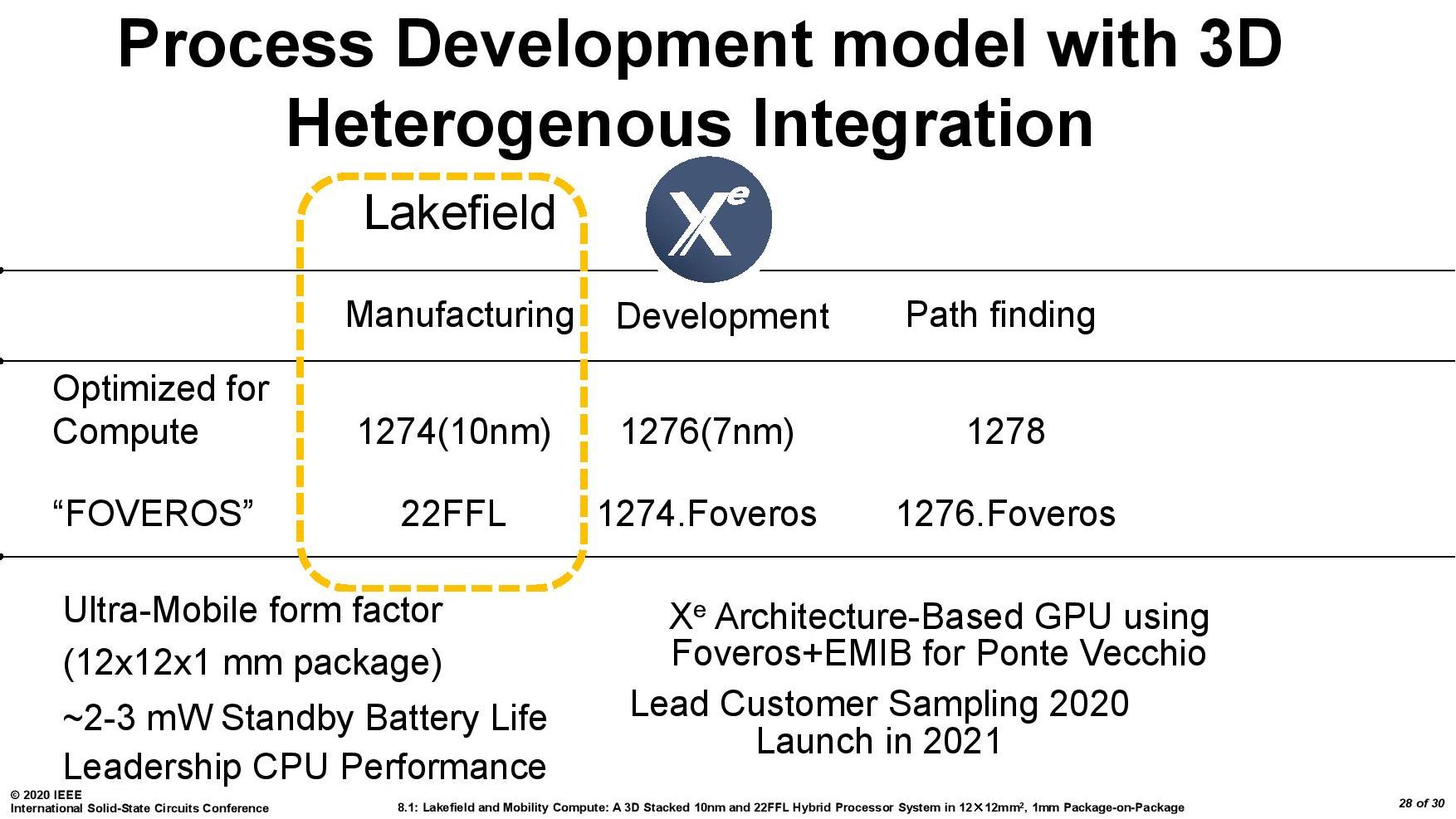
This slide essentially states that Lakefield product in the yellow box has two silicon die – one optimized for compute on Intel’s P1274 process (10+ nm) and the Foveros layer (the active interposer layer) on Intel’s 22FFL process.
The next product with heterogeneous manufacturing integration will be Intel’s big Xe-HPC product, Ponte Vecchio, which will use Intel’s P1276 process (7nm) as a compute die and Intel’s P1274 (10+) process as a base interposer layer.
Beyond this, Intel looks to continue with its multi-layered products by having the compute layer on the most advanced process node, with the interposer layer one generation behind, on a ‘Foveros’ optimized variant.
So the first generation Lakefield is essentially a product that combines P1274 and 22FFL, and a future product is likely to be built on P1276 on the compute layer and P1274 for the interposer layer. Keeping this sort of cadence makes a lot of sense. However, Intel is going to have to learn from Lakefield in a number of ways, especially as we look at ways in which the heterogeneous layering concept can expand. I’ve split this into several areas that I feel is critical to where layered processors can really make a difference.
Growing a Stacked Die to Higher TDP and Core Count
I’ve combined these two points because they essentially go together. Implementing two simple silicon die together in a small form factor product, while is interesting on the power side of the equation, doesn’t probe the question of scaling the product up. It’s easy enough to scale the product out by adding in some form of connectivity to the stack and then connecting them together (which is what’s happening in Ponte Vecchio), but at some point the stack has to move to a higher level of power consumption if it wants to move upwards in power.
This means that thermals become a bigger issue if it wasn’t already. If we take the current Lakefield design, with one compute die over an active interposer, with the right routing then moving to a physically larger floorplan and a higher power shouldn’t be too much of an issue – if anything, making the base die larger should help spread a lot of that IO about, making the interposer a functionally less active interposer. Or Intel will implement the next generation of its die-to-die stacking technology, where the top dies can be larger than the base dies, in a cantilevered fashion.
The bigger deal with the thermals is going to be on the top, with the stacked PoP memory. We go more into the memory communications aspect in a bit, but ideally that memory needs to be on the side so the compute die can have access to a proper heatspreader. The only reason it is stacked in Lakefield is because of the size constraints and attempting to get everything into that small form factor. For anything larger, there needs to be a memory controller that looks outside the chip, which is kind of what we’re expecting from Ponte Vecchio with HBM. A desktop-class product would likely be in the middle.
Growing a Stacked Die to More Stacks
The other angle for a stacked silicon product is to put more stacks in place. This again brings about the question on cooling between the stacks, depending on what is actually there. Lakefield is only two stacks right now, with one high-powered stack and one low-powered stack. Intel would have to prove that it could manage multiple high-powered stacks in order to expand compute in the vertical dimension, but that brings about its own problems.
To start, with Lakefield, the main power to the top compute die is provided with TSVs going through the active interposer layer. For each compute die in a multi-die stack, there would have to be TSVs for each one in order to provide individual power. Unless the active interposer also acted as a PMIC, this could become difficult depending on what other TSVs or data paths need to be put in place between the layers.
Note, when we spoke with Intel’s Ramune Nagisetty at IEDM last year, when asked if Intel would ever discuss if a stacked product would use ‘dummy’ layers to help in cooling, we were told that this would unlikely be mentioned, focusing only on the layers that actually do any work. But ultimately there could be cause for dummy layers to aid in cooling, such that they can provide mass and distance between thermal hotspots between compute dies involved. As the number of layers increases, however, something like Lakefield would have to move the PoP memory off the top, as already mentioned.
Memory Communications
One element to the Lakefield design we haven’t really covered here is how the memory communicates. In the current Lakefield design, the compute cores and the memory controllers are located on the compute die. In order for a portion of main memory to be read into the compute die, the communication has to travel down through the active interposer, go into the package, and then loop back up to the stacked memory.
In the following diagram, on the left, we have (1) going from Compute Die to DRAM, and (2) DRAM back to Compute Die.
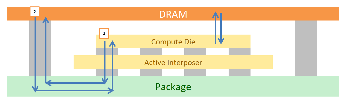
This path is a lot longer than simply going from the compute die straight up into the memory, which would be theoretical on the right hand side if the two were bonded and had appropriate pathways.
If a future Lakefield product wants to continue down the memory-on-top route, one optimization could be to bond that top memory die in a Foveros-like fashion. One could argue that it means Intel would have to bond the memory on at the manufacturing stage, but this already happens with the current generation of Lakefield designs. The only downside would be getting the bonding pads on the top of the compute die and the bottom of the memory die to line up, and then manage the communications from there. The power for the memory would have to also come through on TSVs.
But if we’re bonding the memory into the stack, then technically it could go at any layer – there are likely benefits to keeping the compute die/dies on top. This could lead to multiple layers of memory as needed.
Power Management
With the current Lakefield design, both the compute die and the active interposer die have their own power management IC (PMICs) in order to help deliver power. Based on Intel’s own diagrams, these PMIC designs take up more physical PCB space than Lakefield itself.
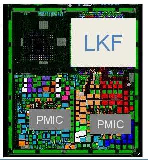
At some level, Intel is going to have to figure out to create a unified PMIC solution to cover every layer on the product. It likely reduces board space and would make things a lot simpler, as it does with laptops that can manage power to the CPU and GPU on the same die with an onboard power controller. A PMIC that can scale with layer counts is obviously going to be a plus.
Cooling
Through all of this, as I’ve mentioned several times, cooling is going to be a major concern. There’s no easy way around the physics of dissipating 5-10 W in such a small space, or over 100 W if the product scales up into something in a form factor that has a wider appeal. Previously in the article I mentioned that we had discussed this with Intel, and how areas such as microfluidic channels have obviously had some research put into, but nothing to the point where it could be done commercially and at scale. It’s a paradigm worth solving, because the benefits would be tremendous.
Beyond Windows and Enabling 5G
One thing to note is that Intel's Lakefield is only planned with Windows 10 support right now. Linux is currently not in the plan for this product, but it would have to be if Intel wants wider adoption of the technology.
Not only this, but as most people are comparing these devices to Qualcomm's hardware, appropriate 5G support will need to be applied - the current generation Lakefield is not part of Intel and Mediatek's collaboration on 5G, which only applies to Tiger Lake and beyond. Lakefield customers will have to rely on 4G as an optional extra, or 5G through an external modem.
The Future Of Lakefield
Even if this first generation version of Lakefield gets slammed pretty hard in performance-focused benchmark reviews for being slower than a dual-core Whiskey Lake, Lakefield marks some very big steps for Intel. Hybrid CPU designs, and stacked die-to-die connectivity, are going to feature in Intel’s future roadmaps – at what points will depend on how much Intel is willing to experiment but also how well Intel can execute. There have been discussions on Intel perhaps looking at an 8+8 hybrid CPU design in the future, although nothing we can substantiate, but we do know that Ponte Vecchio with stacked die is coming in late 2021.
One of the key ingredients in all of this is going to be at what points Intel’s technology portfolio is going to intersect its product portfolio. Some of these technologies might find their way better suited to aspects such as 5G networking, or automotive, rather than something we can consume on the desktop. As far as Lakefield goes, this first generation is going to be a rough challenge for Intel – they are pitching a low performance product in a high-cost segment based on technology (and to a certain extent, battery life). Die-to-die stacking will get easier to do as scale ramps, and hopefully new process node technologies will drive the power efficiency of those big cores lower to enable 2+4 or bigger designs when in a stacked form factor.
We eagerly await a chance to test 1st Gen Lakefield, but we’re also keeping an eye on what might be in the second and third generations.


221 Comments
View All Comments
ichaya - Sunday, July 19, 2020 - link
SPEC is useful for some IPC comparisons, but it's questionable to use it for much else. PG bench in the phoronix link has a 50%+ speedup with SMT which is basically inline for perf/W/$ with Graviton 2 instance. The worst case is Casandra, but everything else is within ~5% for similar perf/$ if not comparable perf/W too since comparing TDP is workload dependent as well and not measured by most tests.XZ and Blender are ~45% faster with SMT in your openbenchmark link, but that's a 3900X (12-core/24-thread), so any comparisons to server chips (64-core Graviton 2) are unfair given power consumption and core differences. 4 times the L3 is also wrong, it's 50% more L2+L3 with half the cores and SMT if you're being fair between m6g.16xlarge or c6g.16xlarge and c5a.16xlarge.
Quantumz0d - Friday, July 3, 2020 - link
Intel has lost it's edge. And this whole portable nonsense is reaching peaks of stupidity. Those Lakefield processor equipped machines will be close to $1000 for their thin and ultra light 1 USB C / 1 3.5mm audio jack, what a fucking disaster.I had owned one ultrabook which is Acer Aspire S3 and I used to even play DotA2 on that, and after 1-2 years the whole machine heated like crazy, I repasted, no dice, cleaned fans, nothing. And then battery also stopped holding a charge. Now what ? That stupid POS is dead, not even worth, meanwhile a Haswell machine with rPGA socket, and an MXM slot from 2013 and guess what ? the GPU got an upgrade to Pascal 1070 MXM from Kepler 860M.
All these BGA trash machines will no longer hold charge nor have their serviceability, older ultrabooks atleast had a 2.5" drive, newer ones have NVMe SSDs, these 2 in 1 trash like most of the Surface lineup is almost impossible to even repair or service. And because of this thin and light market Windows 10 has been ruined as well to cater to this bs phenomenon and desktop class OS is hit with that ugly Mobile UX which lacks powerful software options, navigation and all. Plus you don't even get to repair it yourself due to non available servicing parts.
With Apple HW same thing, full BGA not even NVMe SSDs, and now they also started to make their Mac OS look and feel like iOS trash. This whole mobile and ultra portable garbage is ruining everything, from gaming to the HW.
PandaBear - Monday, July 6, 2020 - link
They don't want to cannibalize their highly profitable x86 business, so they have to give you crap for what you want if you want to pay less. The problem right now is other companies don't have to deal with this political monopoly BS and they are eating Intel for lunch.Most monopolies die this way: when their monopoly business is obsoleted and they hang on to it to milk the cow till it dies.
yeeeeman - Friday, July 3, 2020 - link
Tigerlake should also be in the pipeline soon, right?Deicidium369 - Saturday, July 4, 2020 - link
Benchmarks showing it destroying AMD Renoir at single core, and within 17% on MT - despite half the cores...https://wccftech.com/intel-10nm-core-i7-1165g7-cpu...
watzupken - Sunday, July 5, 2020 - link
"Benchmarks showing it destroying AMD Renoir at single core, and within 17% on MT - despite half the cores...https://wccftech.com/intel-10nm-core-i7-1165g7-cpu...
Till we see the actual performance, you need to take these leaks with a lot of salt. The test bed are not revealed in leaks and it is not possible to ascertain if it is a realistic number. This we don't have to speculate for long since it should be out pretty soon.
pugster - Friday, July 3, 2020 - link
Lakefield's 2.5w standby sounds kind of high. ARM cpu is probably much lower than that.Ian Cutress - Monday, July 20, 2020 - link
2.5 mWProDigit - Friday, July 3, 2020 - link
Qualcomm has proven that a single fast core isn't enough. Intel needs to at least do 2 fast cores. Then add at least 6 atom cores.But if Intel wants to compete with AMD, it'll need to create a quad core big setup, with at least 10 to 12 atom cores.
Any less will be too little. These are too little as is, competing against the 3000 series of AMD.
It would be awesome, if Intel could make a 25W quad core cpu, paired with an additional 40 watts on atom cores. That's about 20 additional cores, or a 24 core cpu.
abufrejoval - Friday, July 3, 2020 - link
A great article overall, very informative, deeply technical while still readable to a layman, very little judgement or marketing, allowing readers to form their own opinion: Anandtech at its very best!Not mentioned in the article and not covered by the comments so far is that the main driver behind Intel’s low power SoCs has been Apple: This is what Intel thought Apple would want and be happy with!
And if you contrast it to what Apple will now do on their own, that makes me want to sell all my Intel shares: Good thing I never had any.
This is another Intel 80432 or i860, tons of great ideas engineered into parts, but great parts don’t automatically make a convincing whole.
And I simply don’t see them iterate that into many more designs over the next years at competitive prices: With that hot-spot governed layout between the two all the flexibility and cost savings a chiplet design is supposed to deliver goes away and you now have two chips in a very tight symbiosis with no scale-up design benefits.
It’s a Foveros tech demo, but a super expensive one with very little chance of currying favors even at ‘negative revenues’ in the current market.
X86 is not competitive in terms of Watts or transistors required for a given amount of compute. It didn’t matter that much in PCs, the competing servers were much worse for a long time, but in the mobile space, phones to ultrabooks, it seems impossible to match ARM, even if you could rewind the clock by ten years and started to take BIG-little seriously. Lakefield is essentially a case study for Core being too big and thus power hungry and Atom failing on performance.
ISA legacy is still holding x86 from dying completely, but that matters less and less at both the top of the performance range with servers and at the bottom in mobile, where the Linux kernel rules supreme and many userlands and ISAs compile just fine.
Gaming is a hold-out, but perhaps the last generation consoles on x86, gamer PCs alone too much of a niche to determine the future.
The desktop will switch to who offers the bigger, longer lasting bang for the buck and there is a very good chance that will be ARM next.
Microsoft may be allowed to blunder along with lackluster ARM64 support for a couple more days, but Apple’s switch puts them under long deserved pressure. A nice Linux/Android/Chromium hybrid ultrabook running whatever Office could get things moving quicker… at least I hope that, because I’d never want to be forced into the bitten Apple…. by these corporate decision makers I see already twitching.
No chance I’d ever let a new Apple into my home: The ][ was the last good one they made.