The Intel Lakefield Deep Dive: Everything To Know About the First x86 Hybrid CPU
by Dr. Ian Cutress on July 2, 2020 9:00 AM ESTLakefield in Terms of Laptop Size
In a traditional AMD or Intel processor designed for laptops, we experience two to eight processing cores, along with some graphics performance, and it is up to the company to build the chip with the aim of hitting the right efficiency point (15 W, or 35/45 W) to enable the best performance for a given power window. These processors also contain a lot of extra connectivity and functionality, such as a dual channel memory controller, extra PCIe lanes to support external graphics, support for USB port connectivity or an external connectivity hub, or in the case of Intel’s latest designs, support for Thunderbolt built right into the silicon without the need for an external controller. These processors typically have physical dimensions of 150 square millimeters or more, and in a notebook, when paired with the additional power delivery and controllers needed such as Wi-Fi and modems, can tend towards the board inside the system (the motherboard) totaling 15 square inches total.
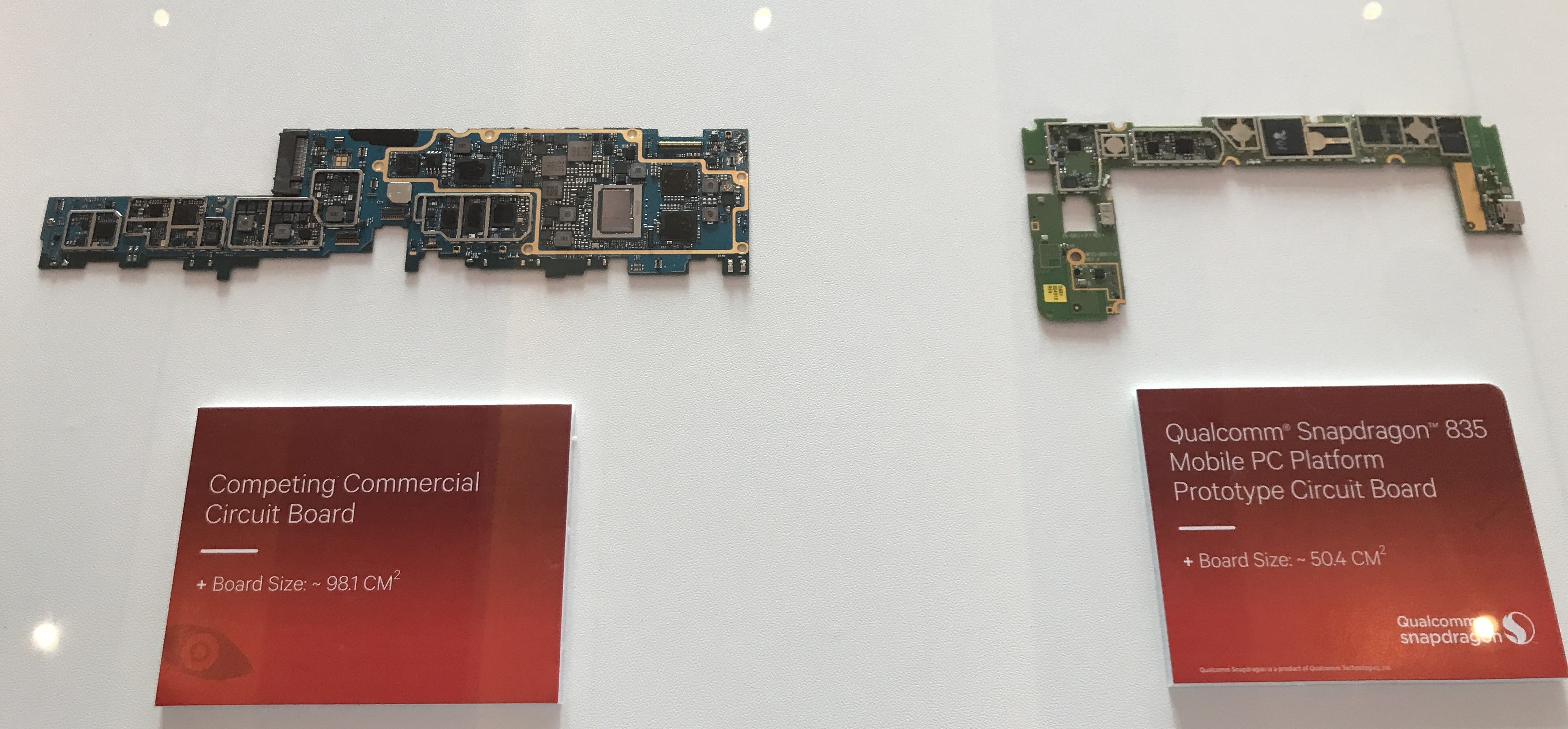
One of Qualcomm’s examples from 2018
For a Qualcomm processor designed for laptops, the silicon is a paired down to the essentials commonly associated with a smartphone. This means that modem connectivity is built into the processor, and the hardware associated with power delivery and USB are all on the scale of a smartphone. This means a motherboard designed around a Qualcomm processor will be around half the size, enabling different form factors, or more battery capacity in the same size laptop chassis.
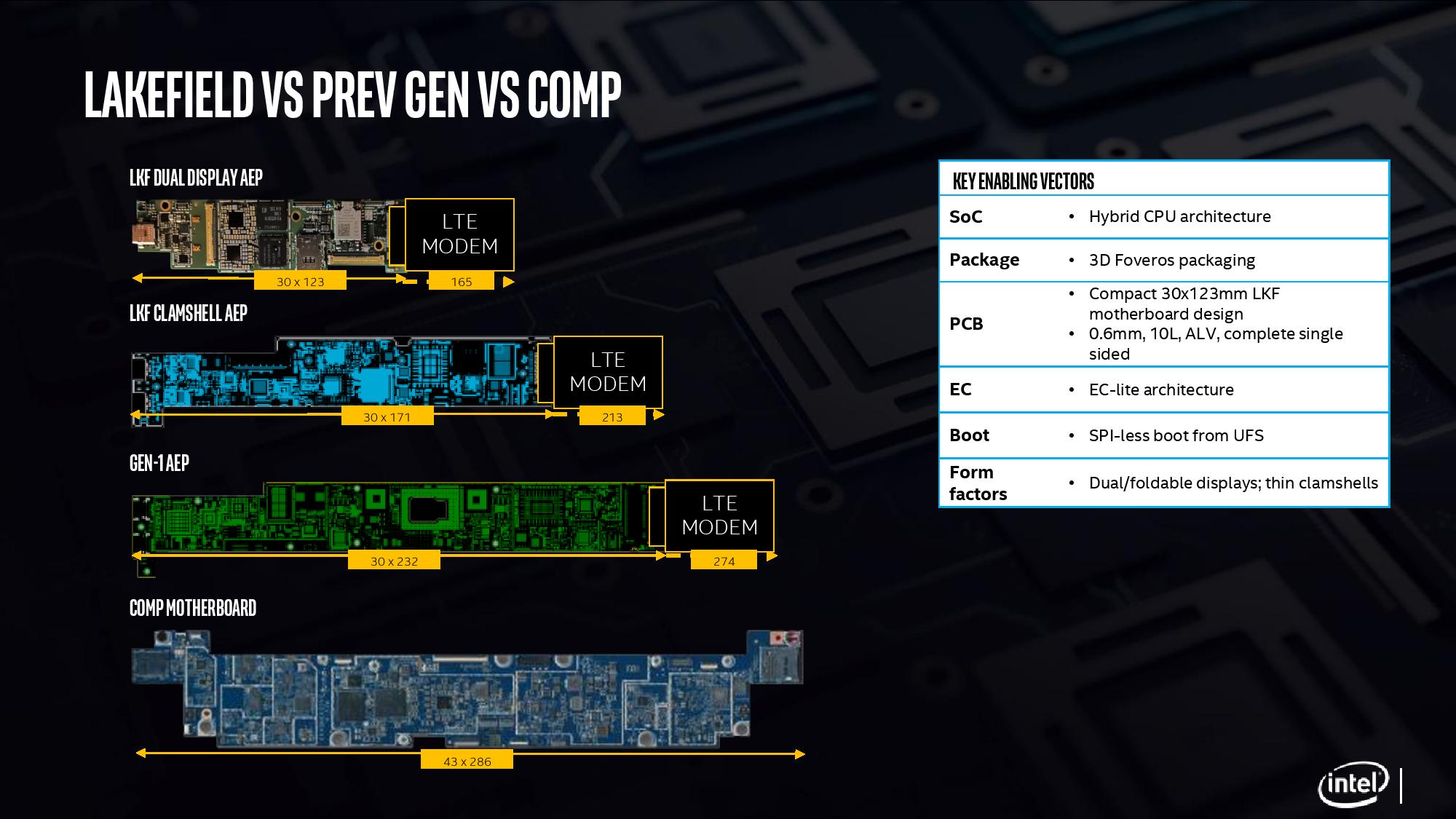
With Intel’s new Lakefield processor design, the chip is a lot smaller than previous Intel implementations. The company designed the processor from the ground up, with as much included on the CPU as to not need additional chips on the motherboard, and to fit the dimensions similar to one of Qualcomm’s processors. Above is a slide showing how Intel believes that with an LTE modem included, a Lakefield motherboard can move down to 7.7 square inches, similar to a Qualcomm design. This leaves more room for battery inside a device.
When Intel compares it against its own previous low power CPU implementations, the company quotes a 60% decrease in overall board area compared to its first generation 4.5 W processors.
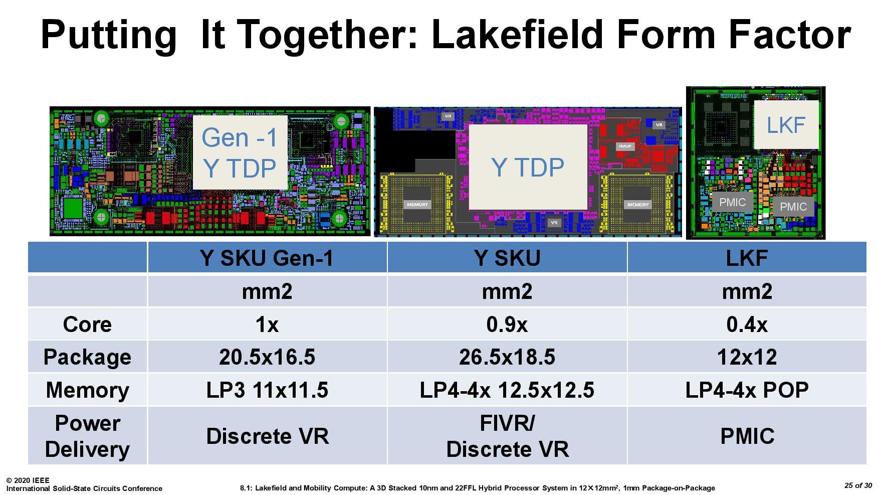
It is worth noting that for power delivery, Intel placed MIMCAPs inside the Lakefield silicon, much like a smartphone processor, and as a result it can get by on the power delivery implementation with a pair of PMICs (power management ICs). The reason why there is two is because of the two silicon dies inside – they are controlled differently for power for a number of technical reasons. If each layer within an active stacked implementation requires its own PMIC, that would presumably put an upper limit on future stacked designs – I fully expect Intel to be working on some sort of solution for this for it not to be an issue, however that wasn’t implemented in time for Lakefield.
For those that are interested, Lakefield’s PMICs are under the codenames Warren Cove and Castro Cover, and were developed in 2017-2018.


221 Comments
View All Comments
extide - Thursday, July 2, 2020 - link
It's 22FFL, which is a derivative of the 14nm process.ProDigit - Friday, July 3, 2020 - link
All chip manufacturers make CPUs at variable lithography. Even AMD. When it says their Ryzens are built on a 7nm node, it means 7nm is the smallest, but other parts still use 10, 12, 14 or 22 nm.Ryzen 2000 CPUs had parts still running on 28nm.
FunBunny2 - Friday, July 3, 2020 - link
"other parts still use 10, 12, 14 or 22 nm. Ryzen 2000 CPUs had parts still running on 28nm."which raises a question, which I suppose is answered somewhere in the hardware engineering space: I suppose having multiple 'node' sizes on the same line is possible due to the fact that the native 'node' is way larger than, in this case, 7nm by multi-masking, and backing off on masks to print the larger 'node' segments. so, if we should ever get to some Xnm, say 7nm, as native resolution, would the machinations to print up, say 28nm, be more work than the current process of printing down?
bji - Thursday, July 2, 2020 - link
Very likely you meant 0.2 PICOjoules of energy consumed per bit, not 0.2 PETAjoules.JayNor - Thursday, July 2, 2020 - link
Someone from Intel mentioned that they have a chiplet version of their LTE modem that can go in the stacked design. I don't recall where the interview is, though...Deicidium369 - Thursday, July 2, 2020 - link
https://tech.hindustantimes.com/tech/news/intel-s-... makes mention of Lakefield and an LTE modem."chiplet" is a marketing term.
Ian Cutress - Monday, July 20, 2020 - link
We asked that with our interview with Ramune Nagisetty from Intel. They say they can do it, but it's not done here.brucethemoose - Thursday, July 2, 2020 - link
Theres potential for another Micron partnership here, as Intel needs custom stackable DRAM dies with TSVs that they can stick below a compute die. Going through the package and back up to memory with a long, narrow interface seems like a tremendous waste of power.And That 4-atom cluster takes up as much space as a AVX-less sunny cove die... a bunch of those would be interesting in a reticle size or EPYC-style Xeon. Cloud providers subdivide giant Xeons into smaller instances anyway, and I imagine that many customers would prefer 4 full cores for the same cost as a single hyperthreaded one. Thats more or less what AWS is pitching with their Graviton chips.
nandnandnand - Thursday, July 2, 2020 - link
Just imagine a 256-core Gracemont or later Atom CPU using chiplets. That could be great for servers.That's basically a return to Xeon Phi, except those cores were modified to do AVX-512.
brucethemoose - Thursday, July 2, 2020 - link
Indeed. In hindsight, Intel designed and pushed Phi towards the wrong market.