The Intel Lakefield Deep Dive: Everything To Know About the First x86 Hybrid CPU
by Dr. Ian Cutress on July 2, 2020 9:00 AM ESTLakefield in Terms of Laptop Size
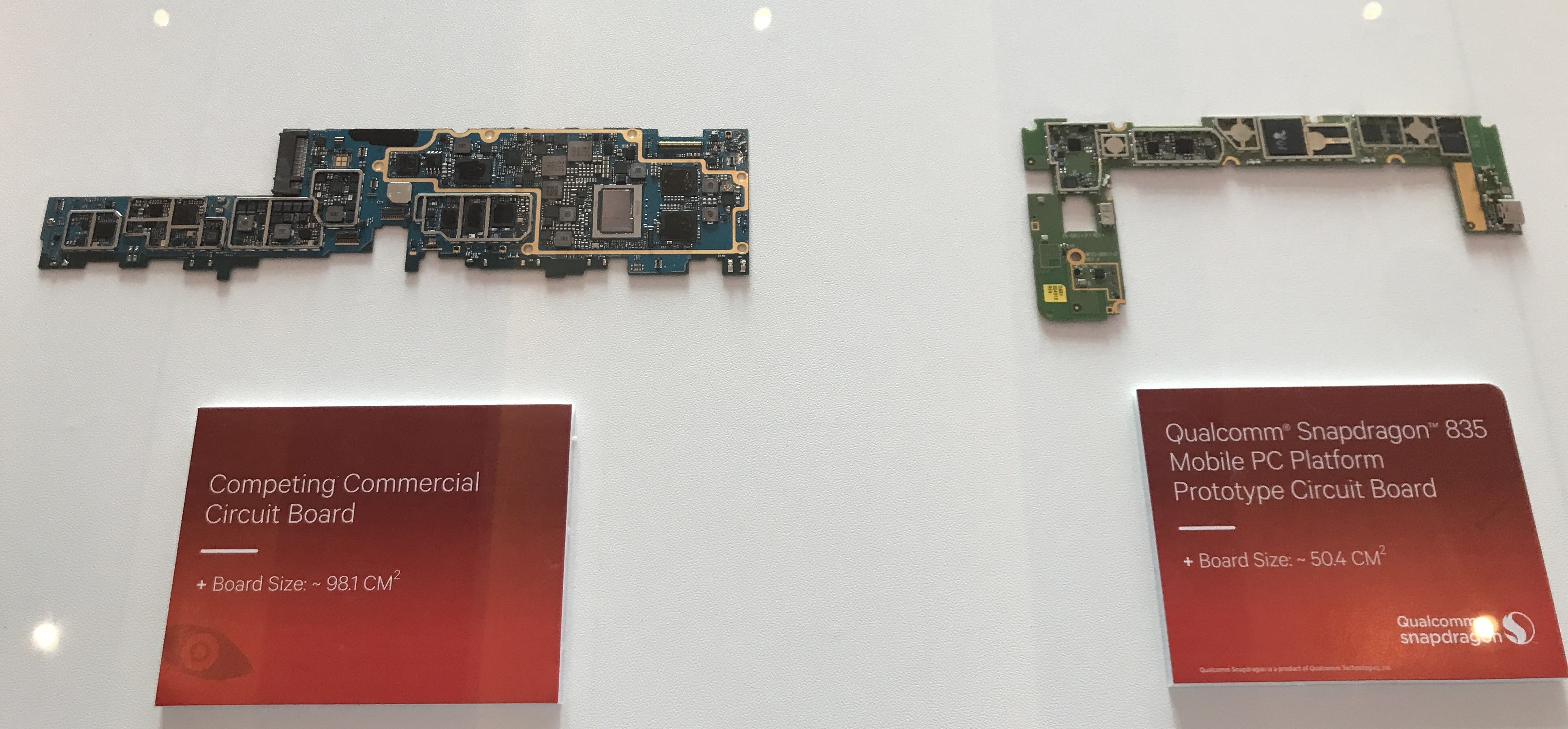
In a traditional AMD or Intel processor designed for laptops, we experience two to eight processing cores, along with some graphics performance, and it is up to the company to build the chip with the aim of hitting the right efficiency point (15 W, or 35/45 W) to enable the best performance for a given power window. These processors also contain a lot of extra connectivity and functionality, such as a dual channel memory controller, extra PCIe lanes to support external graphics, support for USB port connectivity or an external connectivity hub, or in the case of Intel’s latest designs, support for Thunderbolt built right into the silicon without the need for an external controller. These processors typically have physical dimensions of 150 square millimeters or more, and in a notebook, when paired with the additional power delivery and controllers needed such as Wi-Fi and modems, can tend towards the board inside the system (the motherboard) totaling 15 square inches total.
One of Qualcomm’s examples from 2018
For a Qualcomm processor designed for laptops, the silicon is a paired down to the essentials commonly associated with a smartphone. This means that modem connectivity is built into the processor, and the hardware associated with power delivery and USB are all on the scale of a smartphone. This means a motherboard designed around a Qualcomm processor will be around half the size, enabling different form factors, or more battery capacity in the same size laptop chassis.
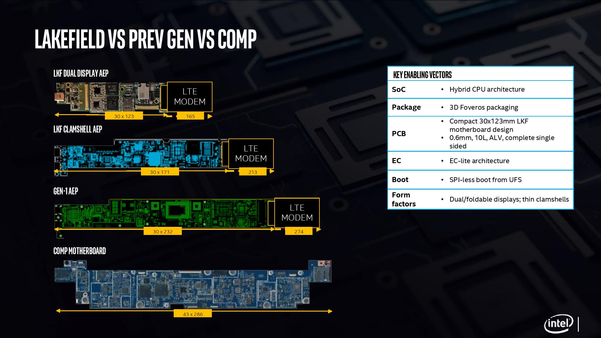
With Intel’s new Lakefield processor design, the chip is a lot smaller than previous Intel implementations. The company designed the processor from the ground up, with as much included on the CPU as to not need additional chips on the motherboard, and to fit the dimensions similar to one of Qualcomm’s processors. Above is a slide showing how Intel believes that with an LTE modem included, a Lakefield motherboard can move down to 7.7 square inches, similar to a Qualcomm design. This leaves more room for battery inside a device.
When Intel compares it against its own previous low power CPU implementations, the company quotes a 60% decrease in overall board area compared to its first generation 4.5 W processors.
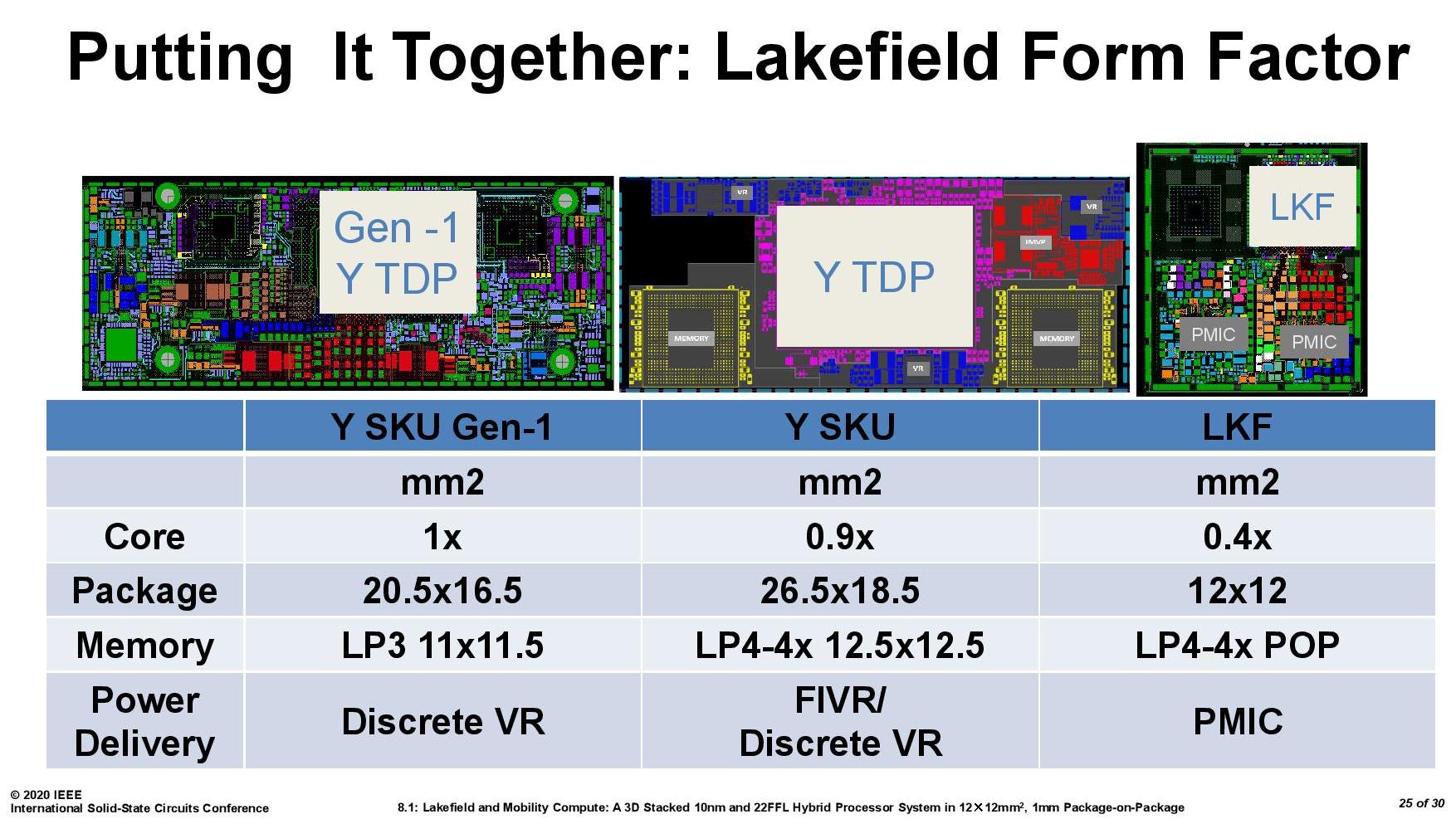
It is worth noting that for power delivery, Intel placed MIMCAPs inside the Lakefield silicon, much like a smartphone processor, and as a result it can get by on the power delivery implementation with a pair of PMICs (power management ICs). The reason why there is two is because of the two silicon dies inside – they are controlled differently for power for a number of technical reasons. If each layer within an active stacked implementation requires its own PMIC, that would presumably put an upper limit on future stacked designs – I fully expect Intel to be working on some sort of solution for this for it not to be an issue, however that wasn’t implemented in time for Lakefield.
For those that are interested, Lakefield’s PMICs are under the codenames Warren Cove and Castro Cover, and were developed in 2017-2018.


221 Comments
View All Comments
Spunjji - Monday, July 6, 2020 - link
That's the exact impression I got, too. They seems to be jumping around waving "look, we can do this too" when really it would have made far more practical sense *not to do it*.watzupken - Sunday, July 5, 2020 - link
Conceptually, this is a good way to lower power requirements to make Intel more competitive against ARM SOCs. However I agree that this is indeed for part smartphone, and part PC. Which unfortunately also means it may not be good for either one. From a smartphone perspective, while this may be a low power chip, but I am still not convinced that an x86 chips can be as efficient as a high end ARM chip. On the PC/ laptop space, I feel it will be more economical to just go for the pure Tremont based chips which should offer sufficient performance for light chores, and still offer good battery life. In my opinion, this is going to be a very niche chip and likely won't be cheap either.Farfolomew - Monday, July 6, 2020 - link
The engineers for this got screwed over by the marketing teams. There is no way this is supposed to compete with higher-end Core chips. It's supposed to be the New Atom replacement: It's supposed to fix everything that was wrong with previous 0+4 Atom CPUs: sluggish OS response and, to an extent, slow single-threaded perf. And also a boost in GPU capabilities.I hope Intel doesn't abandon this, even though, as Ian said, this first gen is going to get slammed
serendip - Tuesday, July 7, 2020 - link
I think Intel should have gone the other way by bringing Sunny Cove idle power down to ARM levels, instead of making this Frankenstein's monster of a chip. ARM licensees all use big cores to speed up UI threads and OS response but Intel seems to be using little Tremont Atom cores for everything. An upgrade to Atom wouldn't have saved Intel's position in mobile, not when ARM big cores have higher perf/watt.PandaBear - Monday, July 6, 2020 - link
Did I see $2499 for the Lenovo? Holy smoke, it is going to fail with this kind of processor. I think Intel is doomed with this being done on 10nm.hanselltc - Monday, July 6, 2020 - link
How does Comet lake fit into that power/performance graph?qwertymac93 - Monday, July 6, 2020 - link
Those performance numbers have me shaking my head. Currently, the chip is acting more like a "1 OR 4" core, not a "1 AND 4" core design. I can't help but wonder if two "big" cores would have been both faster and more power efficient... Clearly this product is suffering from first-gen-itus. 2021 can't come soon enough for Intel.MS - Tuesday, July 7, 2020 - link
Another science project by someone who has a stake in the Atom design. Some things are so bad, it's impossible to kill them. Avoton, Covington, they were all terrible products and all you need to do is look at the performance/power graph to see that there isn't even a net power saving. It's like putting a Pinto engine into a Mustang and expecting better gas mileage. What are they thinking? Or are they? The only thing they missed is piggy backing a Larrabee.name99 - Tuesday, July 7, 2020 - link
"here’s what Intel did, with each connection operating at 500 mega-transfers per second. The key point on this slide is the power: 0.2 picojoules of energy consumed per bit transferred."It's worth comparing this to the competition. TSMC has LIPINCON which is not exactly identical (I don't believe TSMC has publicly demo'd a stacked version) but at the abstract level of "chiplet to chiplet communication" it's the same thing.
TSMC gets 0.56pJ of power, but at a substantially faster 8GT/s. I don't know the extent to which this would scale down if reduced to Intel speeds, and whether its energy costs would go down (or even up, but that seems unlikely) if it were operating vertically rather than horizontally through an RDL.
Point is Foveros is a branding more than a technology per se. It's Intel's way of performing a particular type of packaging, but as far as we can tell, the same style of packaging is available to anyone who uses eg TSMC, if it met their particular goals.
(So far it hasn't because Apple, QC, Huawei, etc, can fit their entire SoC on a single die, they don't need to go through these contortions to either reduce the die size or deal with the limited capabilities of their fabs...
That sounds snarky, but Lakefield is deeply fishy. Sure, you want to save area, but the target is a tablet, and Apple's tablet SoC's have been 120 to 150mm^2. You'd figure a single die Lakefield all on 10nm would fit in ~150mm62 or less. So???)
And Samsung? I would guess so, but I don't know.
Spunjji - Friday, July 10, 2020 - link
Apple aren't trying to squeeze all of their profit margins out of the CPU alone, though. That's the difference.This is Intel trying to preserve margins by using fancy packaging technology to increase yield (and thus both output and margins) on their increasingly capacity-constrained nodes.