The Intel Lakefield Deep Dive: Everything To Know About the First x86 Hybrid CPU
by Dr. Ian Cutress on July 2, 2020 9:00 AM ESTLakefield in Terms of Laptop Size
In a traditional AMD or Intel processor designed for laptops, we experience two to eight processing cores, along with some graphics performance, and it is up to the company to build the chip with the aim of hitting the right efficiency point (15 W, or 35/45 W) to enable the best performance for a given power window. These processors also contain a lot of extra connectivity and functionality, such as a dual channel memory controller, extra PCIe lanes to support external graphics, support for USB port connectivity or an external connectivity hub, or in the case of Intel’s latest designs, support for Thunderbolt built right into the silicon without the need for an external controller. These processors typically have physical dimensions of 150 square millimeters or more, and in a notebook, when paired with the additional power delivery and controllers needed such as Wi-Fi and modems, can tend towards the board inside the system (the motherboard) totaling 15 square inches total.
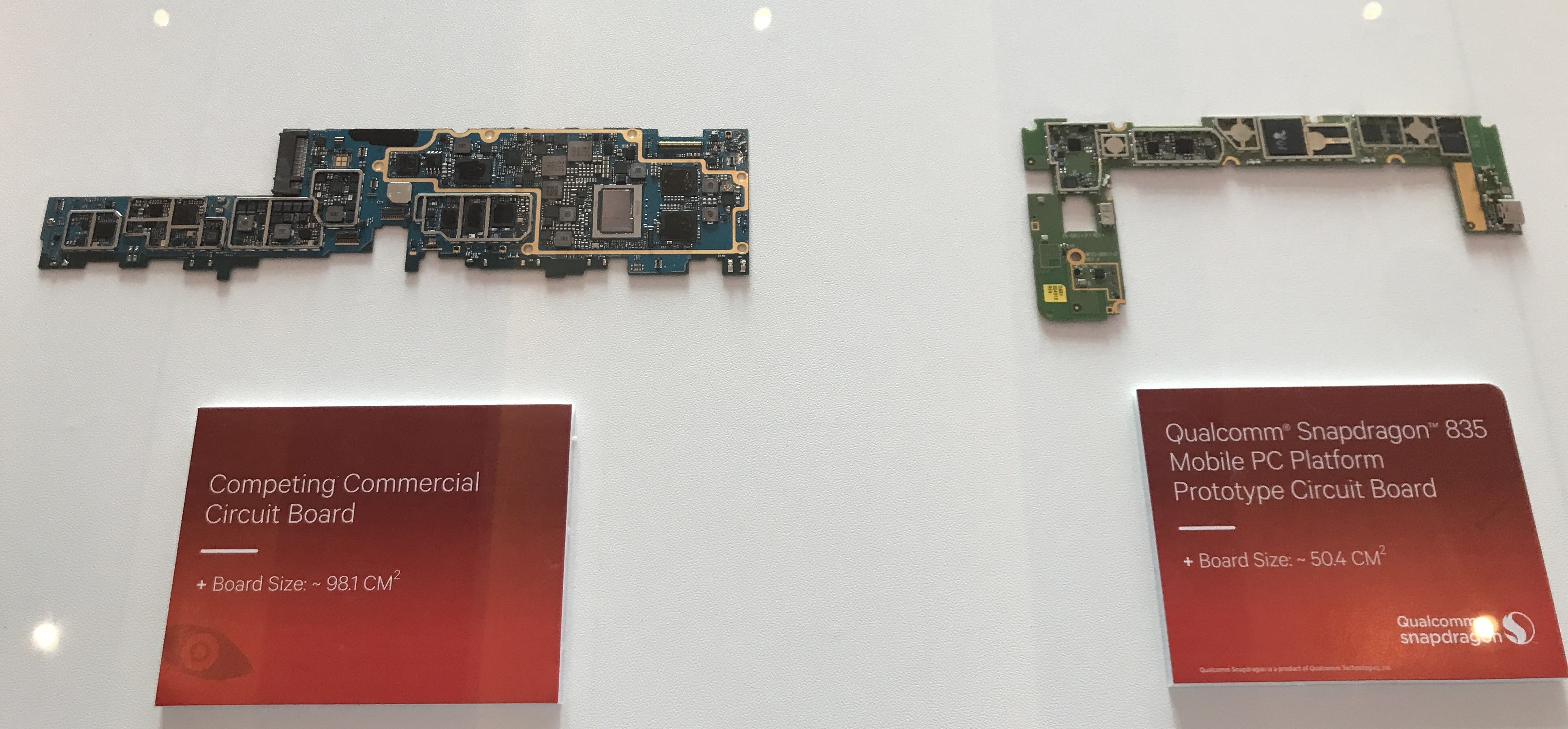
One of Qualcomm’s examples from 2018
For a Qualcomm processor designed for laptops, the silicon is a paired down to the essentials commonly associated with a smartphone. This means that modem connectivity is built into the processor, and the hardware associated with power delivery and USB are all on the scale of a smartphone. This means a motherboard designed around a Qualcomm processor will be around half the size, enabling different form factors, or more battery capacity in the same size laptop chassis.
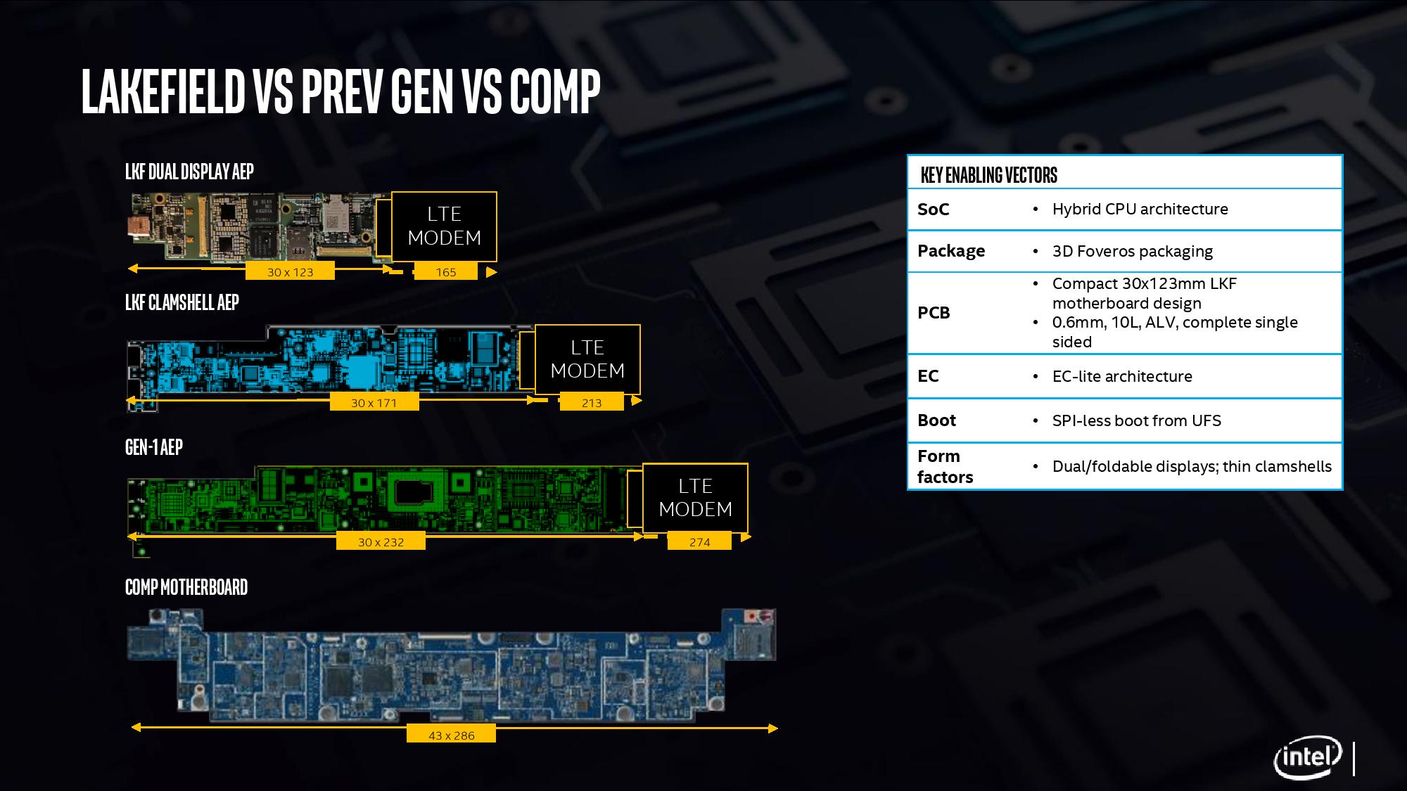
With Intel’s new Lakefield processor design, the chip is a lot smaller than previous Intel implementations. The company designed the processor from the ground up, with as much included on the CPU as to not need additional chips on the motherboard, and to fit the dimensions similar to one of Qualcomm’s processors. Above is a slide showing how Intel believes that with an LTE modem included, a Lakefield motherboard can move down to 7.7 square inches, similar to a Qualcomm design. This leaves more room for battery inside a device.
When Intel compares it against its own previous low power CPU implementations, the company quotes a 60% decrease in overall board area compared to its first generation 4.5 W processors.
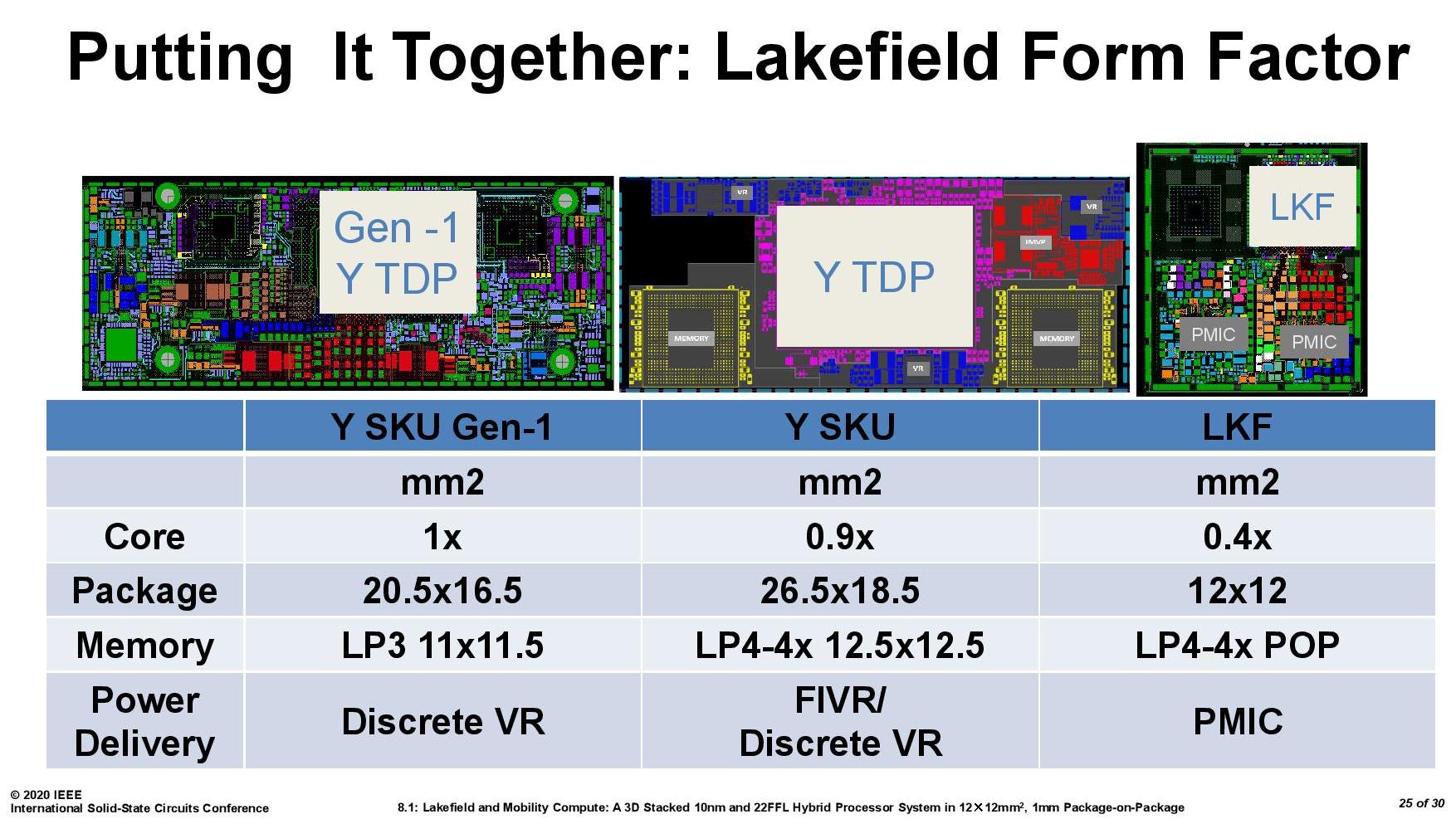
It is worth noting that for power delivery, Intel placed MIMCAPs inside the Lakefield silicon, much like a smartphone processor, and as a result it can get by on the power delivery implementation with a pair of PMICs (power management ICs). The reason why there is two is because of the two silicon dies inside – they are controlled differently for power for a number of technical reasons. If each layer within an active stacked implementation requires its own PMIC, that would presumably put an upper limit on future stacked designs – I fully expect Intel to be working on some sort of solution for this for it not to be an issue, however that wasn’t implemented in time for Lakefield.
For those that are interested, Lakefield’s PMICs are under the codenames Warren Cove and Castro Cover, and were developed in 2017-2018.


221 Comments
View All Comments
PaulHoule - Saturday, July 4, 2020 - link
@DrK,the engineering on this part is like what you'd get if you contracted out to Rockwell or Litton Industries for a brain for a Stinger missile. Compact, brilliantly packaged, with adequate performance, but no concern at all about thermal dissipation because the missile is going to hit or miss its target before the CPU fries.
Foveros is an expensive technology for a mass market device (cheap tablet) because the fabrication cost depends on the total area and there is an expensive step of stitching the chips together at the end. If you could avoid fabricating "glue" components and just snap together chips from a library this might be an amazing technology to build 500 of something at low development cost and time (e.g. weeks) If you have to make a new mask for the chip, however, it is a lot less fun.
So far as AVX the problem is as you say: "who cares about AVX?" Intel has shipped a backlog of features that people don't use because of overhead and complexity. As a software dev I get paid to work on certain aspect of my products, and maximizing performance with the latest instructions may or may not be on my agenda. If it is easy to do I will push for it but it means debugging compatibility problems it is a tough ask. "Optimal" performance for a range of users can mean shipping many versions of a function; the performance of loading, installing, updating, those libraries will be not in the least optimal.
Intel is like that Fatboy Slim album, 'We're #1, Why Try Harder?' The world has changed and Intel is not the #1 CPU firm any more. Intel has to get more Paranoid or it might not Survive.
Spunjji - Monday, July 6, 2020 - link
Why start with "I'm not one to criticise" and then do it? Clearly you are, and as a rhetorical flourish it's tedious in the extreme.1 - It's a first-gen product and it shows, but they're putting it in premium products.
2 - No deep-dive, for sure, but Intel's own figures are not very encouraging.
3 - Citation needed here. There's no sign of it being used outside of low-power premium devices.
4 - Who cares about AVX indeed! Tell that to the Intel fanboys pissing all over the AMD threads?
I'm entirely in favour of your final conclusion, but it's not really supported by the previous statements. 🤷♂️
Oxford Guy - Friday, July 3, 2020 - link
Bricklake or bust.Meteor2 - Friday, July 3, 2020 - link
Ultimately this is another attempt by Intel to stay relevant in a space where it's always struggled: mobile. With the progress being made by Apple, Microsoft, and Qualcomm using ARM, Intel is looking at losing an ever-growing chunk of what was the laptop market.But whatever Intel tries, bottom line is that ARM is more efficient than x86.
Beaver M. - Friday, July 3, 2020 - link
Thats not the issue. The issue is that theres not much software in that sector for x86.Valantar - Sunday, July 5, 2020 - link
A few errors in the article: 2 16-bit channels of LPDDR4X should be 2 32-bit channels of LPDDR4X, given that Renoir (with 4 32-bit LP4X channels at the same clock speed) delivers exactly 2x the bandwidth. Right?You should also proofread the pasted-in laptop descriptions; a lot of stuff in them clashes with the previous text.
Beyond that though: great article! Part of the reason why I love AT is for these technical yet understandable deep-dives. Looking forward to the next one.
Pixelpusher6 - Sunday, July 5, 2020 - link
Interesting choice to place the DRAM right over the core, seems like it would make more sense to move it next to the chip but on package. I guess my question is was it worth the complexity to implement this Foveros design to save a little space? It seems like they could have gotten the same benefit by using a traditional packaging i.e. with a little large package. Can you imagine paying $2500 like the price of that Lenovo and having Atom-esque performance?Pixelpusher6 - Sunday, July 5, 2020 - link
*largerFarfolomew - Monday, July 6, 2020 - link
Agreed on the DRAM placement. It seems really out of place. Another "dime size" piece of silicon right next to the Lakefield CPU doesn't seem like it would take up much more board space, and would alleviate a ton of the heat dissipation problems by allowing the compute-layer die to be directly connected to a heatsinkserendip - Monday, July 6, 2020 - link
It seems to be an interesting technical answer to a question nobody asked. Board space is a lot cheaper than what Lakefield would cost. It could also cost more for Intel to produce and they'd be stuck carrying multiple RAM SKUs.Heat dissipation could be a major issue. The slow chip could become even slower if it has to constantly throttle down because of thermal loads. Intel is sadly mistaken if this is supposed to be an ARM competitor.