Examining Intel's Ice Lake Processors: Taking a Bite of the Sunny Cove Microarchitecture
by Dr. Ian Cutress on July 30, 2019 9:30 AM EST- Posted in
- CPUs
- Intel
- 10nm
- Microarchitecture
- Ice Lake
- Project Athena
- Sunny Cove
- Gen11
Thunderbolt 3: Now on the CPU*
One of the big failures of the Thunderbolt technology since its inception has been its adoption beyond that Apple ecosystem. In order to use it, both the host and the device needed TB controllers supplied by Intel. It wasn’t until Thunderbolt 3 started to use USB Type-C, and Thunderbolt 3 having enough bandwidth to support external graphics solutions, that we started to see the number of available devices start to pick up. The issue still remains that the host and device need an expensive Intel-only controller, but the ecosystem was starting to become more receptive to its uses.
With Ice Lake, that gets another step easier.
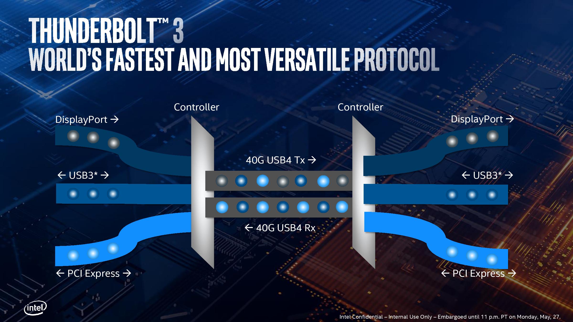
Rather than bundle TB3 support into the chipset, Intel has integrated it on the die of Ice Lake, and it takes up a sizable amount of space. Each Ice Lake CPU can support up to four TB3 ports, with each TB3 port getting a full PCIe 3.0 x4 root complex link internally for full bandwidth. (For those keeping count, it means Ice Lake technically has 32 PCIe 3.0 lanes total).
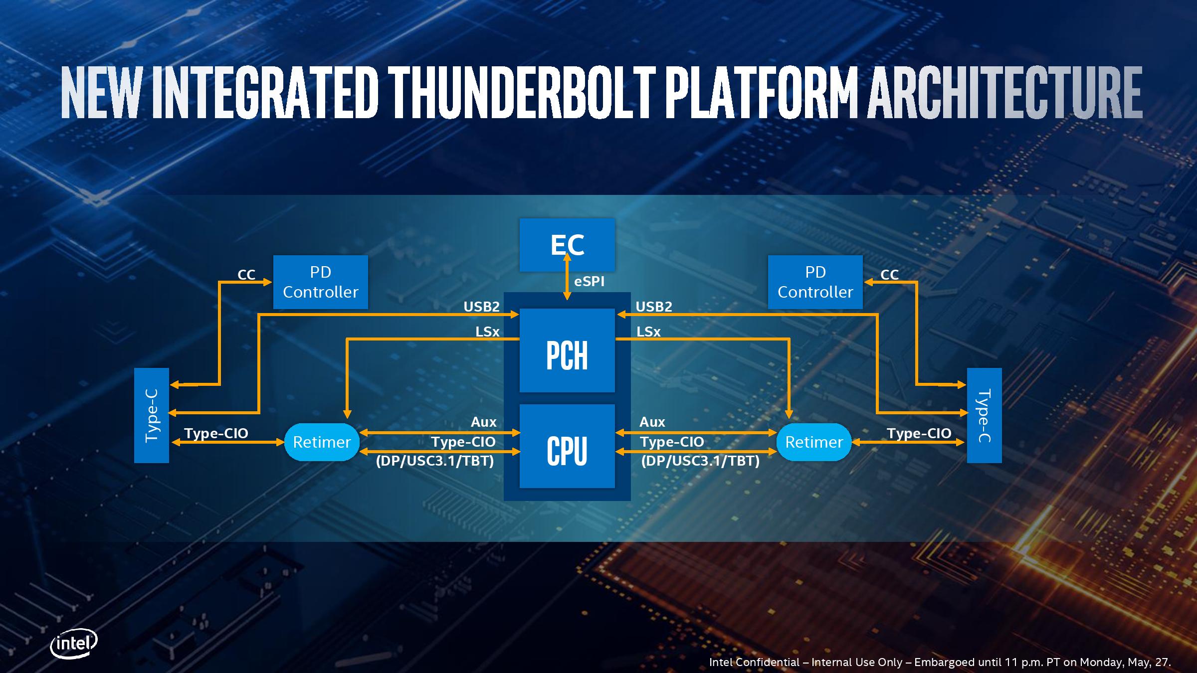
Intel has made it so each side of the CPU can support two TB3 links direct from the processor. There is still some communication back and forth with the chipset (PCH), as the Type-C ports need to have USB modes implemented. It’s worth noting that TB3 can’t be directly used out of the box, however.
Out of the four ports, it will be highly OEM dependent on how many of those will actually make it into the designs – it’s not as simple as just having the CPU in the system, but other chips (redrivers) are needed to support the USB Type-C connector. Power delivery too requires extra circuitry, which costs money. So while Intel advertises TB3 support on Ice Lake, it still needs something extra from the OEMs. Intel states that a retimer for the integrated solution is only half the size compared to the ones needed with the TB3 external chips, as well as supporting two TB3 ports per retimer, therefore halving the number of retimers needed.
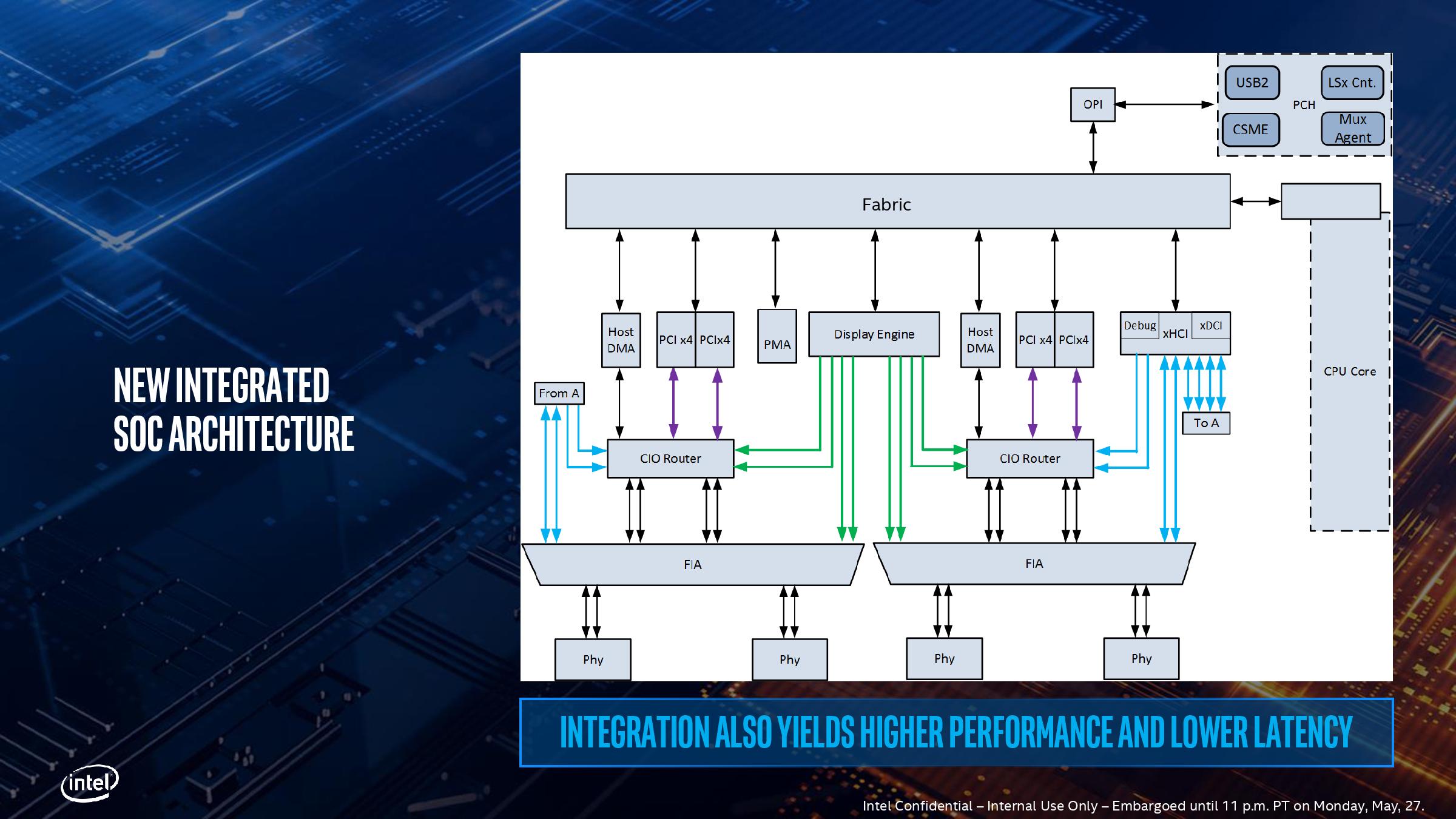
Here’s a more detailed schematic, showing the complexities of adding in TB3 into a chip, with the four PCIe x4 complexes shown moving out to each of the individual PHYs at the bottom, and connected back into the main SoC interconnect fabric. The display engine also has to control what mode the TB3 ports are in, and what signals are being sent. Wake up times for TB3 in this fashion, according to Intel, are actually slightly longer compared to a controller implementation, because the SoC is so tightly integrated. This sounds somewhat counterintuitive, given that the requisite hardware blocks are now closer together, but it all comes down to power domains – in a separate chip design, each segment has a separate domain with individual power up/down states. In an integrated SoC, Intel has unified the power domains to reduce complexity and die area, which means that more careful management is required but latency ultimately increases a little bit.
The other upside to the tightly coupled integration is that Intel stated that this method of TB3 is a lot more power efficient that current external chip implementations. However they wouldn’t comment on the exact power draw of the TB3 block on the chip as it corresponds to the full TDP of the design, especially in relation to localized thermal density (Intel was initially very confused by my question on this, ultimately saying that the power per bit was lower compared to the external chip, so overall system power was lower – they seemed more interested in discussing system power over chip power). Intel did state that the difference between an idle and a fully used link was 300 mW, which suggests that if all four links are in play, we’re looking at 1.2 W. When asked, Intel stated that there are three different power delivery domains within the TB3 block depending on the logic, that the system uses integrated voltage regulation, and the TB3 region has an internal power rail that is shared with some of the internal logic of the CPU. This has implications when it comes to time-to-wake and idle power, but Intel believes it has found a good balance.
Regarding USB4 support, Intel stated that it is in the design, and they are USB4 compliant at this point, but there might be changes and/or bugs which stop it from being completely certified further down the line. Intel said that it ultimately comes down to the device side of the specification, although they have put as much in as they were able given the time constraints of the design. They hope to be certified, but it’s not a guarantee yet.
Depending on who you speak to, this isn’t Intel’s first crack at putting TB3 into CPU silicon: the chip that Intel never wants to talk about, Cannon Lake, supposedly also had an early TB3 design built inside that never worked. But Intel is confident in its Ice Lake implementation, especially with supporting four ports. I wouldn’t be surprised if this comes to desktop when Intel releases its first generation 10nm desktop processors.
*The asterisk in the title of this page is because you still need external hardware in order to enable TB3.


107 Comments
View All Comments
name99 - Wednesday, July 31, 2019 - link
That’s an idiotic chain of reasoning.ARM Macs will ship with macOS, not iOS. To believe otherwise only reveals that you know absolutely nothing of how Apple thinks.
As for comparison, the rough number is A12X gets ~5200 on GB4, Intel best (non-OC’d) gets ~5800. That’s collapsing lots of numbers down to one, but comparing benchmark by benchmark you see Apple does very well (almost matching Intel) across an awful lot.
If Apple can maintain its past pace (and there is no reason why not...) we can expect A13X to be anywhere from 20% to 35% faster, which puts it well into “fastest [non-OC’d] CPU on earth” territory for most single-threaded use cases. Can they achieve this? Absolutely.
Just process improvement can get them 10% frequency. I expect A13X to clock around 2.8GHz.
Then there is LPDDR5 which I expect they will be using, so substantially improved memory bandwidth. Then I expect they'll have SVE (2x256) and accompanying that basically double the bandwidth all the way out from L1 to DRAM.
These are just the obvious basics. There are a bunch of things they can still do that represent “fairly easy” improvements to get to that 25% or so. (These include more aggressive fusion, a double-pumped ALU, attached ALUs to load/store to allow load-ok and op-store fusion, a micro-op cache, long-term-parking, criticality prediction, ...)
So, if it’s so easy, why doesn’t Intel also do it? Why indeed? That’s why I occasionally post my alternative rant about how INTC is no longer an engineering company, it is now pretty much purely a finance company...
ifThenError - Friday, August 2, 2019 - link
Sorry, but both these comments seem mighty uninformed. The MacBooks Air and Pro currently and in the foreseeable future all run on Intel CPUs. The Apple Chips A12/13 are used in iPhone, iPad and the likes.And regarding your prediction, your enthusiasm seems way over the top. What are you even talking about? Micro-op cache on a RISC processor? Think again. Aren't RISC commands all micro ops already?
name99 - Sunday, August 4, 2019 - link
Strong the Dunning-Kruger is with this one...Dude, seriously, learn something about MODERN CPU design, more than just buzz-words from the 80s.
To get you started, how about you read
https://www.anandtech.com/show/14384/arm-announces...
and concentrate on understanding EVERY aspect of what's being added to the CPU and why.
Note in particular that 1.5K Mop cache...
More questions to ask yourself:
- Why was 80s RISC obsessed with REDUCED instructions?
- Why was ARM (especially ARMv8) NOT obsessed with that? Look at the difference between ARMv8 and, say, RISC-V.
- Why is op-fusion so important a part of modern high performance CPUs (both x86 and ARM [and presumably RISC-V if they EVER ship a high-performance part, ha...])?
- which are the fast (shallow logic, even if it's wide) and which are the slow (deep logic) parts of a MODERN pipeline?
ifThenError - Monday, August 5, 2019 - link
Oh my, this is so entertaining you should charge for the reading.You demand to go beyond just buzz words (what would be good) while your posts look like entries to a contest on how many marketing phrases can be fit into a paragraph.
Then you even manage to combine this with highly rude idiom. Plus you name a psychological effect but fail to transfer it to self-reflexion. And as cherry on the top you obviously claim for yourself to understand „EVERY aspect“ of a CPU (an unimaginably complex bit of engineering) but even manage to confuse micro- and macro-op cache and the conceptual differences of these.
I'm really impressed by your courage. Publicly posting so boldly on such a thin basis is brave.
Your comments add near zero information but are definately worth the read. Pure comedy gold!
Please see this as an invitation to reply. I'm looking forwards to some more of your attempts to insult.
Techgeek43 - Tuesday, July 30, 2019 - link
Fantastic article Ian, I for one, cannot wait for ice lake laptopsWonderful in-depth analysis, with an interesting insight into the Intel brand
repoman27 - Tuesday, July 30, 2019 - link
"The high-end design with 64 execution units will be called Iris Plus, but there will be a ‘UHD’ version for mid-range and low-end parts, however Intel has not stated how many execution units these parts will have."Ah, but they have: Ice Lake-U Iris Plus (48EU, 64EU) 15 W, Ice Lake-U UHD (32EU) 15 W. So their performance comparisons may even be to the 15 W Iris Plus with 64 EUs, rather than the full fat 28 W version.
I know you have access to the media slide decks, but Intel has also posted product briefs for the general public that contain a lot of this info: https://www.intel.com/content/www/us/en/products/d...
"On display pipes, Gen11 has access to three 4K pipes split between DP1.4 HBR3 and HDMI 2.0b. There is also support for 2x 5K60 or 1x 4K120 with a 10-bit color depth."
The three display pipes are not limited to 4K, and are agnostic of transport protocol—each of them can be output via the eDP 1.4b port, one of the 3 DDI interfaces which can support either DisplayPort 1.4 or HDMI 2.0b, or one of the up to 4 Thunderbolt 3 ports. Both HDMI and DP support HDCP 2.2, and DisplayPort also supports DSC 1.1. The maximum single pipe, single port resolution for HDMI is 4K60 10bpc (4:2:2), and for DisplayPort it's 4K120/5K60 10bpc (with DSC).
Thunderbolt 3 integration for Ice Lake-Y is only up to 3 ports.
abufrejoval - Tuesday, July 30, 2019 - link
What I personally liked most about the GT3e (48 EU) and GT4e (72 EU) Skylake variant SoCs was, that they didn't cost the extra money they should have, especially when you consider that the iGPU part completely dwarfs the CPU cores (which Intel makes you bleed for) and is much better than everything else combined together (have a look at the WikiChips layoutshttps://en.wikichip.org/wiki/intel/microarchitectu...
Of course, a significantly better graphics performance is never a bad thing, especially when it also doesn't cost extra electrical power: The bigger iGPUs might have actually been more energy efficient than their GT2 brethren at a graphics load that pushed the GT2 towards its frequency limits. And in any case if you don't crunch it on graphics, the idle consumption is near perfect: One of the reasons most laptop dGPU designs won't even bother to run 2D on the dGPU any more but leave that to Intel.
The biggest downside was that you couldn't buy them outside an Apple laptop or Intel NUC.
But however much Intel goes into Apple mode (the major customer for these beefier iGPUs) in terms of "x time faster than previous", the result aren't going to turn ultrabooks with this configuration into "THD gaming machines".
To have a good feel as to where these could go and whether they are worth the wait, just have a look at the Skull Canyon nuc6i7kyk review on this site: That SoC uses 72 EUs and 128MB of eDRAM and should put a pretty firm upper limit to what a 64 EU Ice Lake can do: Most of the games in that review are somewhat dated yet fail to reach 20FPS at THD.
So if you want to game on the device, you'd be much better of with a dGPU however small and chose the smallest iGPU variant available. No reason to wait, Whisky + Nvidia will do better.
If you want real gaming performance, you need to put real triple digit Watts and the bandwidth only GDDR5/6 or HBM can deliver to work even at THD, but with remote gaming perhaps it doesn't have to be on your elegant slim ultrabook. There again anything but the GT2 configuration is wasted, because only need the VPU part for decoding Google Stadia (or Steam Remote) streams, which is the same for all configurations.
For some strange reason, Intel has been selling GT3/4 NUCs at little or no premium over GT2 variants and in that case I have been seriously tempted. And only once I even managed to find a GT3e laptop once for a GT2 price (while the SoC is literally twice as big and the die carrier even adds eDRAM at zero markup), which I stil cherish.
But if prices are anywhere related to the surface area of the chip (as they are for the server parts), these high powered GTs are something that only Apple users would buy.
That's another reaons, I (sadly) don't expect them to be sold in anything bug Macs and some NUCs, no ChuWi notebooks or Mini-ITX boards.
abufrejoval - Tuesday, July 30, 2019 - link
...(need edit)Judging from the first 10nm generation, GPUs where the part where obtaining economically feasible yields didn't work out. Unless they have really, really fixed 10nm it's not hard to imagine that Intel could be selling high-count EU SoCs to Apple below cost, to keep them for another generation as flagship customer and perhaps due to long-term contractual obligations.
But maintaining GT2/3/4 price egality for the rest of the market seems suicidal even if you have a fab lead.
Not that I expect we'll ever be told: In near monopoly situations the so called market ecnomy becomes surprisingly complex.
willis936 - Wednesday, July 31, 2019 - link
What the hell is a THD in this context?jospoortvliet - Monday, August 5, 2019 - link
Probably full HD (True HD)?