GlobalFoundries Stops All 7nm Development: Opts To Focus on Specialized Processes
by Anton Shilov & Ian Cutress on August 27, 2018 4:01 PM EST- Posted in
- Semiconductors
- CPUs
- AMD
- GlobalFoundries
- 7nm
- 7LP
GlobalFoundries on Monday announced an important strategy shift. The contract maker of semiconductors decided to cease development of bleeding edge manufacturing technologies and stop all work on its 7LP (7 nm) fabrication processes, which will not be used for any client. Instead, the company will focus on specialized process technologies for clients in emerging high-growth markets. These technologies will initially be based on the company’s 14LPP/12LP platform and will include RF, embedded memory, and low power features. Because of the strategy shift, GF will cut 5% of its staff as well as renegotiate its WSA and IP-related deals with AMD and IBM. In a bid to understand more what is going on, we sat down with Gary Patton, CTO of GlobalFoundries.
7LP Canned Due to Strategy Shift
GlobalFoundries was on track to tape out its clients’ first chips made using its 7 nm process technology in the fourth quarter of this year, but “a few weeks ago” the company decided to take a drastic, strategic turn, says Gary Patton. The CTO stressed that the decision was made not based on technical issues that the company faced, but on a careful consideration of business opportunities the company had with its 7LP platform as well as financial concerns.
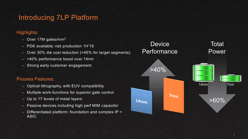
It is noteworthy that when GlobalFoundries first announced its 7LP platform in September 2016, it said that it would start risk production of processors using this technology in early 2018 (PR), which means that the first chips should have been taped out before that. When the company detailed the process in June 2018, it said that it expected to start “volume production ramping in the second half of 2018” (PR), which would be close to impossible if customers taped out their first chips only in Q4.
Generally, it looks like the company had to adjust its roadmap somewhere along the way, moving the start of high-volume manufacturing (HVM) further into 2019. Whether or not these adjustments had any implications on GlobalFoundries is up to debate. Keep in mind that AMD’s first 7 nm product was designed for TSMC’s CLN7FF from the beginning, so the company did not bet on GF’s 7LP in late 2018 anyway, and no rush with the manufacturing technology was needed for GF’s key customer.
Along with the cancellation of the 7LP, GlobalFoundries essentially canned all pathfinding and research operations for 5 nm and 3 nm nodes. The company will continue to work with the IBM Research Alliance (in Albany, NY) until the end of this year, but GlobalFoundries is not sure it makes sense to invest in R&D for ‘bleeding edge’ nodes given that it does not plan to use them any time soon. The manufacturer will continue to cooperate with IMEC, which works on a broader set of technologies that will be useful for GF’s upcoming specialized fabrication processes, but obviously it will refocus its priorities there as well (more on GF’s future process technologies later in this article).
So, the key takeaway here is that while the 7LP platform was a bit behind TSMC’s CLN7FF when it comes to HVM – and GlobalFoundries has never been first to market with leading edge bulk manufacturing technologies anyway – there were no issues with the fabrication process itself. Rather there were deeper economic reasons behind the decision.
![]()
Economic Reasons Behind the Move
As we noted in our article covering GlobalFoundries's new CEO hire earlier this year, former CEO Sanjay Jha was never able to make the company profitable. His key tasks were to increase GlobalFoundries’s sales, streamline the company in general, and ensure that it executes its roadmap.
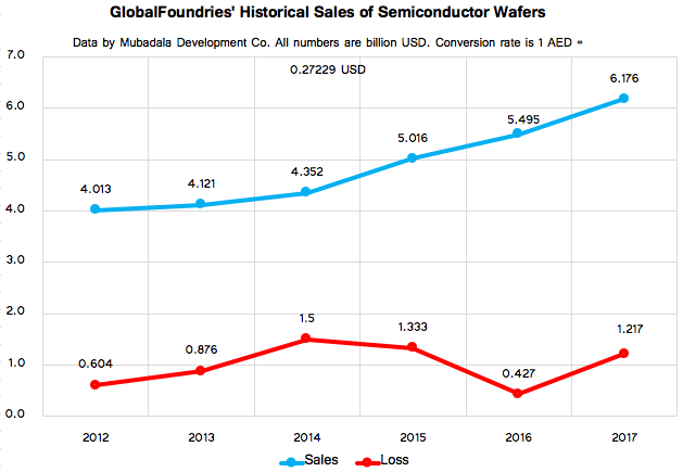
To address the needs of the manufacturer’s traditional key client (AMD) and ensure that his company was competitive against other contract makers of semiconductors, he licensed Samsung Foundry's 14LPP fabrication technology. That strategy worked well. With Sunjay Jha at the helm, GlobalFoundries has managed to land a variety of new customers and increase its sales of semiconductor wafers from approximately $4.121 billion in 2013 to $6.176 billion in 2017. Besides, the foundry’s leading-edge Fab 8, which has been processing wafers using exclusively 14LPP process technology for well over 1.5 years now, is running at full capacity.
To ensure that GlobalFoundries remains competitive against Samsung Foundry and TSMC in the long run, Sunjay Jha obtained IP and development teams from IBM (along with two fabs and a lot of obligations), and poured in billions of dollars in development of the 7LP fabrication technology platform. The latter would include three generations of manufacturing processes and, possibly, a custom high-performance technology available exclusively to IBM. While everything appeared to proceed smoothly with the 1st Gen 7 nm process (DUV only), the 2nd Gen 7 nm process (with EUV used for non-critical layers, such as padding) still needed some additional development investments, and the 3rd Gen 7 nm (with intensive usage of EUV) required even more money for development and further could require installation of additional EUV equipment. Meanwhile, there were two things to consider.
First. If GlobalFoundries kicks off production using the 1st Gen 7 nm fabrication process, it would have needed to cure all of its teething troubles and offer its clients a roadmap forward. The latter would have included 2nd Gen and 3rd Gen 7 nm, but nothing stops there. Customers would have asked for 5 nm and then for 3 nm nodes. Meanwhile, you cannot tell your clients that you are packing up after a certain node and then hope that this node will be a success (the same is true for DUV-only 1st Gen 7 nm).
Second. Development of leading-edge process technologies is extremely expensive. Every new node requires billions of dollars in investments. Those costs are eventually amortized over each chip the company makes, so to keep increasing R&D costs from driving up chip prices, foundries need to produce more chips. To make more chips, they need to either run multiple fabs that use the same process technology (these are going to cost $10+ billion in the EUV era), or build giant fabs that process a gargantuan number of wafers (these are going to cost $20+ billion in the EUV era). Meanwhile, GlobalFoundries has only one leading-edge fab featuring capacity of 60,000 wafer starts per month. As a result, either GlobalFoundries has to pass these R&D costs on to the finite number of wafers it processes – and become uncompetitive against rivals in the process – or eat the costs with reduced profitability.
Meanwhile, having spent well over $20 billion on GlobalFoundries over the last 10 years, Mubadala, the owner of the company, is not inclined to lose more money or invest tens of billions in the hopes of becoming profitable one day. The investor wants GlobalFoundries to stop bleeding and start generating profits.
“The culture of [our investments], the ones I’ve been involved with, was about accumulating assets and then just maintaining it,” said Mubadala CEO Khaldoon Al Mubarak in an interview with Bloomberg earlier this year. “The shift that has happened over the last couple of years, that I’ve tried to push at Mubadala today, is a monetization strategy that makes sense, not with a view to cash out but with a view to reinvest.”
Gary Patton admits that GlobalFoundries never planned to be a leading producer of 7-nm chips in terms of volume. Furthermore, the company has been seeing increasing adoption of its 14LPP/12LP technologies by designers of various emerging devices, keeping Fab 8 busy and leaving fewer step-and-scan systems for 7LP products.
Without another big fab, it would be impossible to make any new leading-edge process technology competitive against Samsung and TSMC due to aforementioned scale reasons. Meanwhile, building a new fab (or even expanding the Fab 8 with another clean room module, which is something that GF considered several years ago) and creating another node or two would require another $10 – $15 billion from Mubadala, which is not inclined to invest just now. As a result, the GlobalFoundries has decided to switch entirely to specialized process technologies for emerging high-growth markets. This strategic shift enables it to reduce spending on R&D, slowdown procurement of new equipment, reduce its workforce by 5% (most of which will be in Malta), and potentially avoid direct competition against the aforementioned contract makers of semiconductors.


127 Comments
View All Comments
drwho9437 - Tuesday, August 28, 2018 - link
The first shoe has dropped.I used to work for IBM Research, though not in the part they sold to Global Foundries, but in the part where they invented the new wrinkles to make better transistors and such. I finished my doctorate in 2012. It was just about a year after I finished that the deal with GF was announced. When this happened I was not sure how much longer IBM would invest in the physical science research for such things. They promised five years I believe. But it made me think about the business case for transistors and I concluded there was not much of a future left.
Simply put quantum effects and statistical effects hurt you more and more as you go smaller, it also blows up in cost. We can debate the end of Silicon scaling till we are blue in the face. Will it be 7 nm or 5 nm or will it be 10-12-14 or something else. It doesn't matter costs go up and amortizing your cost is the better business play at some point.
Can we research something to replace Silicon? Yes. But silicon has 40+ years of investment, you are not likely to invent a technology to overtake it in a few years or for a few dollars. Do you choose to invest in research or driving down the cost of building 14 nm fabs?
I though there would be a break point in 5-6 years where the CEOs would have to choose: amortize or invest a massive amount in researching something totally new. I fully expected them to choose the former. GF just did. Will Intel or Samsung choose differently? I doubt it. Which means a big brick wall is coming. Mr. Moore we have reached the end.
evanh - Tuesday, August 28, 2018 - link
My sole argument is economies of scale is what defines the cost.evanh - Tuesday, August 28, 2018 - link
My sole argument is economies of scale is what defines the cost.Follower - Wednesday, August 29, 2018 - link
If future need to be in our hands, then 7nm drop out may not be a good idea though, as it plays a major role after 5-10 years.richmaxw - Wednesday, August 29, 2018 - link
IBM paid Global Foundries $1.5 billion to take over their foundries. They also gave them patents. In return, Global Foundries said they would provide IBM 10 nm CPUs. How are Global Foundries not in breach of that agreement? AMD is obligated to buy a certain number of CPUs from Global Foundries each year. If they don't buy the minimum amount, they have to pay anyway. But what if Global Foundries is producing out-of-date products? Would AMD have signed that agreement knowing GF was going to just give up on research suddenly? Not only is this decision a waste of the research and development they have already put into 7 nm, it also appears to be dishonest and underhanded to IBM and AMD. I hope they are compensating IBM and AMD for going back on their word.Holliday75 - Wednesday, August 29, 2018 - link
Looking back at previous announcements I am now under the impression that AMD and most likely IBM have known this was coming a long ways off so they could adjust their strategies as needed.As to the agreements in place, if AMD and/or IBM were getting screwed over due to this change I am sure a lawsuit would have already been announced.
Alien959 - Wednesday, August 29, 2018 - link
What i find interesting is that their 7nm process is more or less developed and surly that has some value to someone that has deep pockets and want to be even more vertical integrated like apple. Yes its a huge investment, but does anadtech readership thinks there is a chance that Apple would be interested in getting in the fab business.eastcoast_pete - Wednesday, August 29, 2018 - link
Apple tied itself to TSMC (and vice versa). In return for Apple booking huge quantities and making TSMC their exclusive supplier, TSMC gave Apple first right of refusal for their 7 nm capacity. They both took a risk, but that deal deal gave TSMC what GloFo was missing: a full order book for 7 nm silicon with the attached large, guaranteed revenue stream (many billions of $$$) that made TSMC's investing the necessary multi-billion $$$ into 7 nm tech possible. Right now, I simply don't know any other (fabless) company except Apple that would (or could) sign a two-figure billion dollar purchase order like that; AMD simply doesn't have anywhere near that volume, or the financial muscle, and it looks like even Qualcomm and Huawei had to settle for 7 nm table scraps at TSMC's.While some here have commented on the coming end of Moore's Law, that scenario may have to be amended: in addition to physical limitations to how much one can shrink semiconductor structures, it looks more and more that the costs of shrinking nodes will put the brakes on that development even before we hit the actual physical limits.
@Anandtech: if you guys have the numbers, could you publish a plot of node sizes/nm vs. estimated costs to get a fab up-and-running. This seems to approach an (inverse) exponential function as we go from 14 nm to 10 nm to now 7 nm.
Sahrin - Wednesday, August 29, 2018 - link
GF has been very aggressive in growing the company through private equity acquisition - which means debt, which means interest payments. It'd be interesting to see how the transaction and financing costs of the acquisitions factor into this.GF would not be the first company sunk by ownership's shitty business strategy. Blaming it all on R&D is the idiot's way out. AMD, eg, was sunk by borrowing to buy ATI - not by overspending on R&D.
del42sa - Thursday, August 30, 2018 - link
bunch of loosers....