Sizing Up Servers: Intel's Skylake-SP Xeon versus AMD's EPYC 7000 - The Server CPU Battle of the Decade?
by Johan De Gelas & Ian Cutress on July 11, 2017 12:15 PM EST- Posted in
- CPUs
- AMD
- Intel
- Xeon
- Enterprise
- Skylake
- Zen
- Naples
- Skylake-SP
- EPYC
Intel's New On-Chip Topology: A Mesh
Since the introduction of the "Nehalem" CPU architecture – and the Xeon 5500 that started almost a decade-long reign for Intel in the datacenter – Intel's engineers have relied upon a low latency, high bandwidth ring to connect their cores with their caches, memory controllers, and I/O controllers.
Intel's most recent adjustment to their ring topology came with the Ivy Bridge-EP (Xeon E5 2600 v2) family of CPUs. The top models were the first with three columns of cores connected by a dual ring bus, which utilized both outer and inner rings. The rings moved data in opposite directions (clockwise/counter-clockwise) in order to minimize latency by allowing data to take the shortest path to the destination. As data is brought onto the ring infrastructure, it must be scheduled so that it does not collide with previous data.
The ring topology had a lot of advantages. It ran very fast, up to 3 GHz. As result, the L3-cache latency was pretty low: if the core is lucky enough to find the data in its own cache slice, only one extra cycle is needed (on top of the normal L1-L2-L3 latency). Getting a cacheline of another slice can cost up to 12 cycles, with an average cost of 6 cycles.
However the ring model started show its limits on the high core count versions of the Xeon E5 v3, which had no less than four columns of cores and LLC slices, making scheduling very complicated: Intel had to segregate the dual ring buses and integrate buffered switches. Keeping cache coherency performant also became more and more complex: some applications gained quite a bit of performance by choosing the right snoop filter mode (or alternatively, lost a lot of performance if they didn't pick the right mode). For example, our OpenFOAM benchmark performance improved by almost 20% by choosing "Home Snoop" mode, while many easy to scale, compute-intensive applications preferred "Cluster On Die" snooping mode.
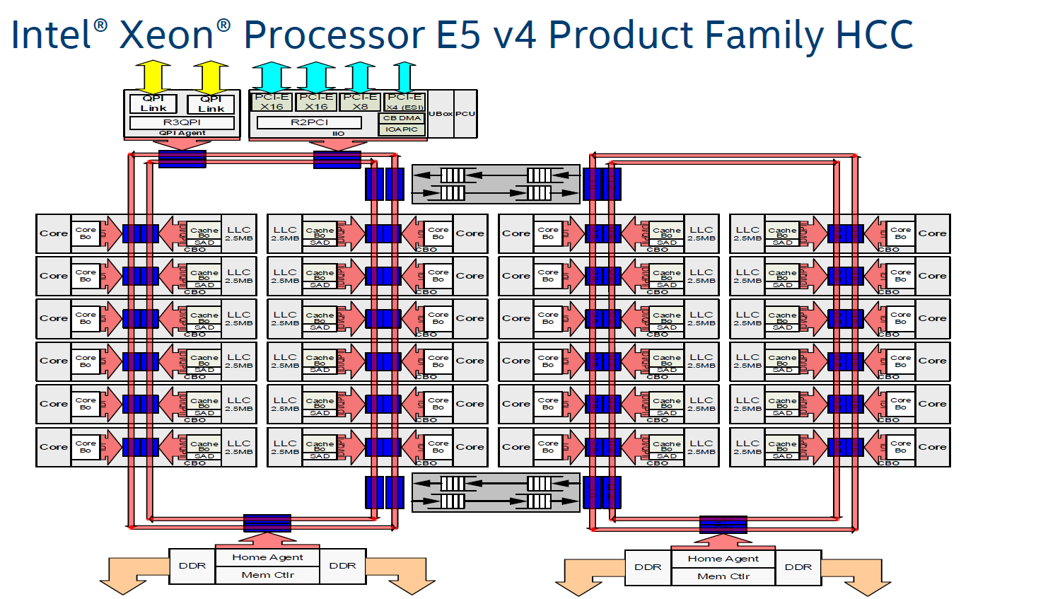
In other words, placing 22 (E7:24) cores, several PCIe controllers, and several memory controllers was close to the limit what a dual ring could support. In order to support an even larger number of cores than the Xeon v4 family, Intel would have to add a third ring, and ultimately connecting 3 rings with 6 columns of cores each would be overly complex.
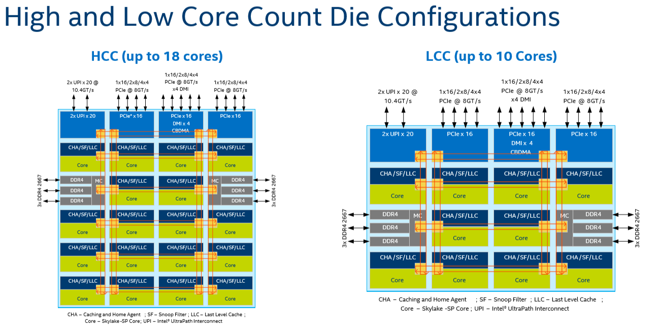
Given that, it shouldn't come as a surprise that Intel's engineers decided to use a different topology for Skylake-SP to connect up to 28 cores with the "uncore." Intel's new solution? A mesh architecture.
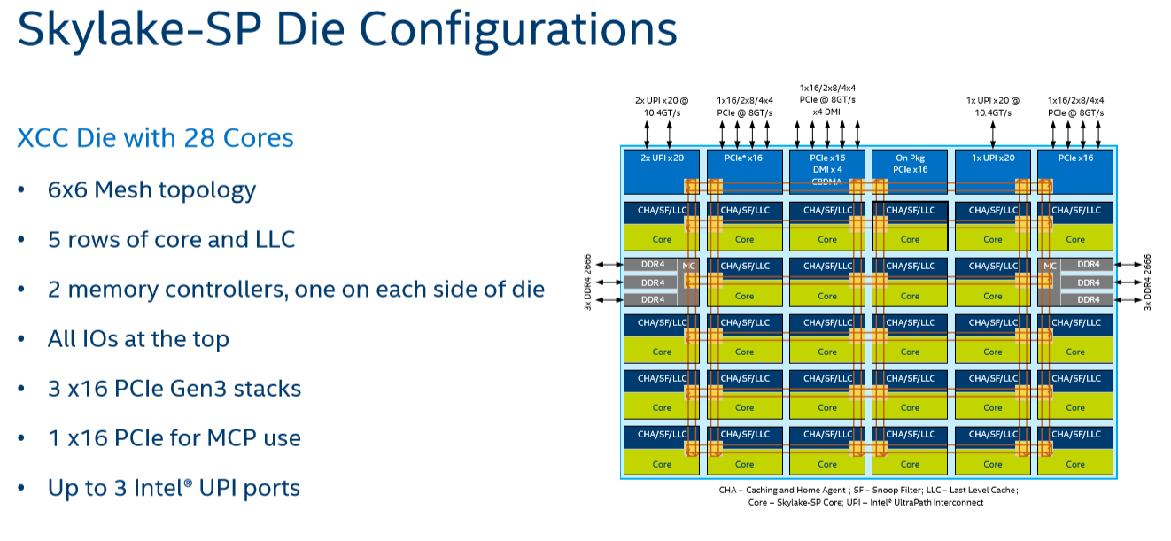
Under Intel's new topology, each node – a caching/home agent, a core, and a chunk of LLC – is interconnected via a mesh. Conceptually it is very similar to the mesh found on Xeon Phi, but not quite the same. In the long-run the mesh is far more scalable than Intel's previous ring topology, allowing Intel to connect many more nodes in the future.
How does it compare to the ring architecture? The Ring could run at up to 3 GHz, while the current mesh and L3-cache runs at at between 1.8GHZ and 2.4GHz. On top of that, the mesh inside the top Skylake-SP SKUs has to support more cores, which further increases the latency. Still, according to Intel the average latency to the L3-cache is only 10% higher, and the power usage is lower.
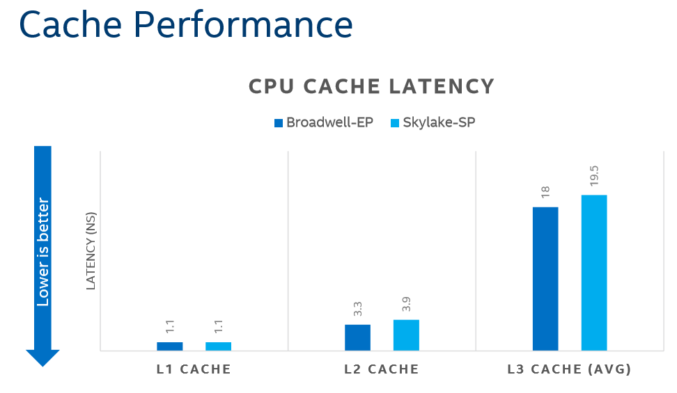
A core that access an L3-cache slice that is very close (like the ones vertically above each other) gets an additional latency of 1 cycle per hop. An access to a cache slice that is vertically 2 hops away needs 2 cycles, and one that is 2 hops away horizontally needs 3 cycles. A core from the bottom that needs to access a cache slice at the top needs only 4 cycles. Horizontally, you get a latency of 9 cycles at the most. So despite the fact that this Mesh connects 6 extra cores verse Broadwell-EP, it delivers an average latency in the same ballpark (even slightly better) as the former's dual ring architecture with 22 cores (6 cycles average).
Meanwhile the worst case scenario – getting data from the right top node to the bottom left node – should demand around 13 cycles. And before you get too concerned with that number, keep in mind that it compares very favorably with any off die communication that has to happen between different dies in (AMD's) Multi Chip Module (MCM), with the Skylake-SP's latency being around one-tenth of EPYC's. It is crystal clear that there will be some situations where Intel's server chip scales better than AMD's solution.
There are other advantages that help Intel's mesh scale: for example, caching and home agents are now distributed, with each core getting one. This reduces snoop traffic and reduces snoop latency. Also, the number of snoop modes is reduced: no longer do you need to choose between home snoop or early snoop. A "cluster-on-die" mode is still supported: it is now called sub-NUMA Cluster or SNC. With SNC you can divide the huge Intel server chips into two NUMA domains to lower the latency of the LLC (but potentially reduce the hitrate) and limit the snoop broadcasts to one SNC domain.


219 Comments
View All Comments
PixyMisa - Tuesday, July 11, 2017 - link
No, the pricing is correct. The 1P CPUs really are half the price of a single 2P CPU.msroadkill612 - Wednesday, July 12, 2017 - link
Seems to me, the simplest explanation of something complex, is to list what it will not do, which they will not do :(.Can i run a 1p Epyc in a 2p mobo e.g., please?
PixyMisa - Thursday, July 13, 2017 - link
Short answer is no. It might boot, but only half the slots, memory, SATA and so on will be available. Two 1P CPUs won't talk to each other.A 2P Epyc will work in a 1P board though.
cekim - Tuesday, July 11, 2017 - link
One glaring bug/feature of AMD's segmentation relative to Intel's is the utter and obvious crippling of clock speeds for all but the absolute top SKUs. Fewer cores should be able to make use of higher clocks within the same TDP envelope. As a result Intel is objectively offering more and better fits up and down the sweep of cores vs clocks vs price spectrum.So, the bottom line is AMD is saying that you will have to buy the top-end, 4S SKU to get the top GHz for those applications in your mix that won't benefit from 16,18,32,128 cores.
I say all of this as someone who desperately wants EPYC to shake things up and force Intel to remove the sand-bags. I know I'm in a small, but non-zero market of users who can make use of dozens of cores, but still need 8 or fewer cores to perform on par with desktop parts for that purpose.
KAlmquist - Wednesday, July 12, 2017 - link
One possibility is that they have only a small percentage of the chips currently being produced bin well enough to be used in the highest clocking SKU's, so they are saving those chips for the most expensive offerings. Admittedly, that depends on what they are seeing coming off the production line. If they have a fair number of chips where with two very good cores, and two not so good, then it would make sense to offer a high clocking 16 core EPYC using chips with two cores disabled. But if clock speed on most chips is limited due to minor registration errors (which would affect the entire chip), then a chip with only two really good cores would require two localized defects in two separate cores, in addition to very good registration to get the two good cores. The combination might be too rare to justify a separate SKU.I would expect Global Foundries to continue to tweak its process to get better yields. In that case, more processors would end up in the highest bin, and AMD might decide to launch a higher clock speed 16 and 8 core EPYC processors, mostly using chips which bin well enough that they could have been used for the 32 core EPYC 7601.
alpha754293 - Tuesday, July 11, 2017 - link
Why does the Intel Xeon 6142 cost LESS than the 6142M? (e.g. per the table above, 6142 is shown with a price of $5946 while the 6142M costs $2949)ca197 - Tuesday, July 11, 2017 - link
I assume that is the wrong way round on the list. I have seen it reported the other way round on other sites.Ian Cutress - Tuesday, July 11, 2017 - link
You're correct. I've updated the piece, was a misread error from Intel's tables.coder543 - Tuesday, July 11, 2017 - link
On page 6, it says that Epyc only has 64 PCIe lanes (available), but that's not correct. There are 128 PCIe lanes per chip. In a 1P configuration, that's 128 PCIe lanes available. On a 2P configuration, 64 PCIe lanes from each chip are used to connect to the other chip, leaving 64 + 64 = 128 PCIe lanes still available.This is a significant advantage.
Ian Cutress - Tuesday, July 11, 2017 - link
You misread that table. It's quoting per-CPU when in a 2P configuration.