Canon Prepares Nanoimprint Lithography Tool To Challenge EUV Scanners
by Anton Shilov on October 17, 2023 12:00 PM EST- Posted in
- Semiconductors
- EUV
- DUV
- NIL
- Canon
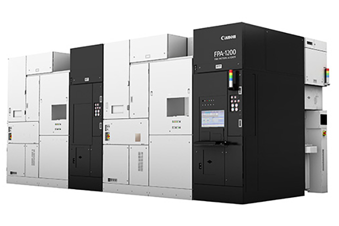
Canon has recently revealed its FPA-1200NZ2C, a nanoimprint semiconductor manufacturing tool that can be used to make advanced chips. The device uses nanoimprint lithography (NIL) technology as an alternative to photolithography, and can theoretically challenge extreme ultraviolet (EUV) and deep ultraviolet (DUV) lithography tools when it comes to resolution.
Unlike traditional DUV and EUV photolithography equipment that transfers a circuit pattern onto a resist-coated wafer through projection, nanoimprint tool employs a different technique. It uses a mask, embossed with the circuit pattern, which directly presses against the resist on the wafer. This method eliminates the need for an optical mechanism in the pattern transfer process, which promises a more accurate reproduction of intricate circuit patterns from the mask to the wafer. In theory, NIL enables formation of complex two- or three-dimensional circuit patterns in a single step, which promises to lower costs. NIL itself is not a new technology, but it has remained in parallel development over the years, while the challenges involved in further improving photolithography have Canon believing that now is a good time for a second-look.
Canon says that its FPA-1200NZ2C enables patterning with a minimum linewidth (critical dimensions, CD) of 14 nm, which is good enough to 'stamp' a circa 26-nm minimum metal pitch, and therefore suitable for 5 nm-class process technologies. That would be in line with capabilities of ASML's Twinscan NXE:3400C (and similar) EUV lithography scanners with a 0.33 numerical aperture (NA) optics.
Meanwhile, Canon says that further refinements of its technology, its tool can achieve finer resolutions that can enable 3 nm and even 2 nm-class production nodes.
Nanoimprint lithography offers several compelling advantages over photolithography. Primarily, NIL excels in resolution, enabling the creation of structures at the nanometer scale with remarkable precision without using photomasks. This technology bypasses the diffraction limits encountered in conventional photolithography, allowing for more intricate and smaller features. Additionally, NIL operates without the necessity of complex optics or high-energy radiation sources, leading to potentially lower operational costs and simpler equipment.
Another advantage of NIL is its direct patterning capability, enabling the reproduction of three-dimensional nanostructures effectively. Such functionality makes NIL a potent tool in the production of photonics and other applications where three-dimensional nano-patterns are essential. The technology also facilitates better pattern fidelity and uniformity.
However, NIL also presents certain challenges and limitations. One notable issue is its susceptibility to defects due to the direct contact involved in the imprinting process. Particles or contaminants present on the substrate or the mold can lead to defects, which may affect the overall yield and reliability of the manufacturing process. This necessitates impeccable process control and cleanliness to maintain consistent output quality.
Additionally, NIL, in its traditional form, is a serial process, which limits its throughput and production capacity. Unlike photolithography, which can process entire wafers or large areas in a parallel fashion, NIL often involves processing smaller areas sequentially. This poses great challenges in scaling the technology for high-volume manufacturing of chips, which limits its usage for chip manufacturing. Meanwhile, NIL can be used to create photomasks for EUV and DUV. Also, it can theoretically be used to create patterned media for hard disk drives.
Source: Canon


14 Comments
View All Comments
name99 - Tuesday, October 17, 2023 - link
"Also, it can theoretically be used to create patterned media for hard disk drives."I like this comment! It suggests a possible economic niche where the tech can get started, and a path to generally available patterned media (which are required for the next big jump in magnetic media capacity).
my_wing - Sunday, October 29, 2023 - link
Sorry I think this is a translation error, my understanding is that it might actually referred to SSD and HDD.The fact that HDD is more like a ribbon, Nanoimprint required a great deal of accuracy to work, I don't think you can cost effectively produce a disk structure i.e. from inside to outside that same shape, think of simple things like printing a T-shirt, how to fill a circle going larger and larger only a square can do it. And HDD has a very large surface compare to CPU let say.
SSD and RAM is what Canon said they target for, largely repeated i.e. using AI and computer, this technology line up right next to the next RAM cell in a continuous manner in increasing capacity. Therefore
"... NIL often involves processing smaller areas sequentially. ..."
The keyword is sequentially, i.e. like you stamp on a maze pattern and you carry on stamping until it create a much larger maze, i.e. more RAM.
The thing that I think Canon should sell to except the plan to Samsung, Micron, etc. (Memory), I think if they can create a mold that is large enough, is to Intel for Backside Power Delivery, I really do think that because of High K material and so on, the thing is difficult but of the back side, it is only coper and some form of non conductive material, the shape is also simple to be imprint, unlike GAA CFET these complex shape can kill imprint, like imprint T-Shirt with multiple colour, but if copper and the insulative material is only 2 colour, then in theory is simpler and compare to ASML nanoimprint is cheaper in total cost of ownership.
Eskimou - Saturday, December 16, 2023 - link
This has been done for years. The compony Canon purchased for the Nanoimprint technology was doing this back in 2009 to print patterned media for HDD companies.https://sst.semiconductor-digest.com/2009/09/hdd-p...
Threska - Tuesday, October 17, 2023 - link
"It uses a mask, embossed with the circuit pattern, which directly presses against the resist on the wafer. "Contact printing.
lefty2 - Tuesday, October 17, 2023 - link
Is this some type of marketing reboot? The FPA-1200NZ2C was released 6 years ago according to this: https://global.canon/en/news/2017/20170720.htmlThe Hardcard - Tuesday, October 17, 2023 - link
That wasn’t a market release, but an announcement that they provided it to Toshiba Memory. What’s new is that it now appears to be generally available.lefty2 - Wednesday, October 18, 2023 - link
not really. other companies were using it 6 years ago: https://semiengineering.com/what-happened-to-nanoi...The Hardcard - Friday, October 20, 2023 - link
No, there is only one Toshiba. Both your links refer to the same machine.Anymoore - Tuesday, October 17, 2023 - link
Canon's NIL is sequentially stepped just like ASML scanners, so there is no serial vs. non-serial.Using NIL for DUV/EUV masks is an interesting proposition, it would actually be harder because the pattern would cover a larger area.
Santoval - Wednesday, November 8, 2023 - link
DUV and in particular EUV masks need to be immaculate though, which is why they are made via the slow but super precise electron beam lithography. Would a defect-prone lithography be suitable for them?A single mask defect would pass that defect in all the printed wafers.