Samsung to Unveil Refined 3nm and Performance-Enhanced 4nm Nodes at VLSI Symposium
by Anton Shilov on May 10, 2023 4:00 PM EST- Posted in
- Semiconductors
- Samsung
- Samsung Foundry
- 3nm
- 4nm
- 3GAE
- 3GAP
- 4HPC
- SF3
- SF4X

Samsung Foundry is set to detail its second generation 3 nm-class fabrication technology as well as its performance-enhanced 4 nm-class manufacturing process at the upcoming upcoming 2023 Symposium on VLSI Technology and Circuits in Kyoto, Japan. Both technologies are important for the contract maker of chips as SF3 (3GAP) promises to offer tangible improvements for mobile and SoCs, whereas SF4X (N4HPC) is designed specifically for the most demanding high-performance computing (HPC) applications.
2nd Generation 3 nm Node with GAA Transistors
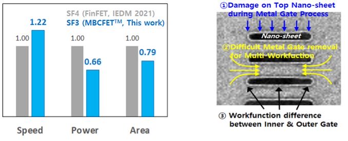
Samsung's upcoming SF3 (3GAP) process technology is an enhanced version of the company's SF3E (3GAE) fabrication process, and relies on its second-generation gate-all-around transistors – which the company calls Multi-Bridge-Channel field-effect transistors (MBCFETs). The node promises additional process optimizations, though the foundry prefers not to compare SF3 with SF3E. Compared to its direct predecessor, SF4 (4LPP, 4nm-class, low power plus), SF3 claims a 22% performance boost at the same power and complexity or a 34% power reduction at the same clocks and transistor count, as well as a 21% logic area reduction. Though it is unclear whether the company has achieved any scaling for SRAM and analogue circuits.
In addition, Samsung claims that SF3 will provide additional design flexibility facilitated by varying nanosheet (NS) channel widths of the MBCFET device within the same cell type. Curiously, variable channel width is a feature of GAA transistors that has been discussed for years, so the way Samsung is phrasing it in context of SF3 might mean that SF3E does not support it.

Samsung's Ealiest 4nm Node: SF4E (IEDM 2021)
Thus far neither Samsung LSI, the conglomerate's chip development arm, nor other customers of Samsung Foundry have formally introduced a single highly-complex processor mass produced on SF3E/3GAE process technology. In fact, it looks like the only publicly-acknowledged application that uses the industry's first 3 nm-class fabrication process is a cryptocurrency mining chip, according to TrendForce. This is not particularly surprising as usage of Samsung's 'early' nodes is typically quite limited.
By contrast, Samsung's 'plus' technologies are typically used by a wide range of customers, so the company's SF3 (3GAP) process is likely to see much higher volumes when it becomes available sometime in 2024.
SF4X for Ultra-High-Performance Applications
In addition to SF3, which is designed for a variety of possible use cases, Samsung Foundry is prepping its SF4X (4HPC, 4 nm-class high-performance computing) designed for performance-demanding applications like datacenter-oriented CPUs and GPUs.
To address such chips, Samsung's SF4X offers a performance boost of 10% coupled with a 23% power reduction. Samsung doesn't explicitly specify what process node that comparison is being made against, but presumably, this is against their default SF4 (4LPP) fabrication technology. To achieve this, Samsung redesigned transistors' source and drain after reassessing their stresses (presumably under high loads), performed further transistor-level design-technology co-optimization (T-DTCO), and introduced a new middle-of-line (MOL) scheme.
The new MOL enabled SF4X to offer a silicon-proven CPU minimum voltage (Vmin) of 60mV, a 10% decrease in the variation of off-state current (IDDQ), guaranteed high voltage (Vdd) operation at over 1V without performance degradation, and an improved SRAM process margin.
Samsung's SF4X will be a rival for TSMC's N3P and N3X nodes, which are due in 2024 and 2025 respectively. Based on claim specificaitons alone, it is hard to tell which technology will offer the best combination of performance, power, transistor density, efficiency, and cost. That said, SF4X will be Samsung's first node in the recent years that was specifically architected with HPC in mind, which implies that Samsung has (or is expecting) enough customer demand to make it worth their time.
Source: Samsung


3 Comments
View All Comments
Threska - Wednesday, May 10, 2023 - link
I can see why everyone's aiming for data-centers, although in Samsung's case there is the cellphone market of which they're right behind Apple. Perfect test bed.https://www.bankmycell.com/blog/us-smartphone-mark...
brucethemoose - Thursday, May 11, 2023 - link
I don’t like those P/X nodes. HPC customers could order chips at slightly lower clocks on the "regular" processes and get a vast reduction in power usage.I get that supply constraints are a factor here too, but still...
dotjaz - Sunday, June 4, 2023 - link
Are you dumb? HPC refers to high clock, AMD use these nodes on Ryzen.