Samsung Announces "X-Cube" 3D TSV SRAM-Logic Die Stacking Technology
by Andrei Frumusanu on August 14, 2020 7:00 AM EST- Posted in
- Samsung Foundry
- TSV
- Packaging
- 3D Packaging
Yesterday, Samsung Electronics had announced a new 3D IC packaging technology called eXtended-Cube, or “X-Cube”, allowing chip-stacking of SRAM dies on top of a base logic die through TSVs.
Current TSV deployments in the industry mostly come in the form of stacking memory dies on top of a memory controller die in high-bandwidth-memory (HBM) modules that are then integrated with more complex packaging technologies, such as silicon interposers, which we see in today’s high-end GPUs and FPGAs, or through other complex packaging such as Intel’s EMIB.

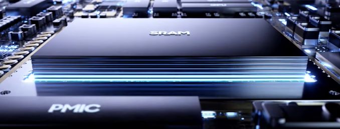
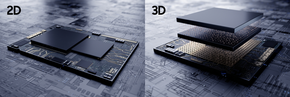
Samsung’s X-Cube is quite different to these existing technologies in that it does away with intermediary interposers or silicon bridges, and directly connects a stacked chip on top of the primary logic die of a design.
Samsung has built a 7nm EUV test chip using this methodology by integrating an SRAM die on top of a logic die. The logic die is designed with TSV pillars which then connect to µ-bumps with only 30µm pitch, allowing the SRAM-die to be directly connected to the main die without intermediary mediums. The company this is the industry’s first design such design with an advanced process node technology.
It’s not the first time that the company has demonstrated TSVs in the base logic die to connect to a stacked die on top of it. Back in 2013, the company had showed custom Exynos chips using Widcon technology, stacking Wide I/O DRAM memory on top of the base logic chip with help of TSVs, offering a higher-performance and lower power solution compared to traditional PoP memory. Unfortunately, this technology never saw the light of day in consumer devices as it likely never was cost-effective enough justify for mass-production.
Stacking more valuable SRAM instead of DRAM on top of the logic chip would likely represent a higher value proposition and return-on-investment to chip designers, as this would allow smaller die footprints for the base logic dies, with larger SRAM cache structures being able to reside on the stacked die. Such a large SRAM die would naturally also allow for significantly more SRAM that would allow for higher performance and lower power usage for a chip.
Samsung’s marketing materials showcase more than a single die of SRAM, which would indicate that X-Cube can be variable in terms of its stack-height. It’s currently unclear if X-Cube will be limited to SRAM dies, or whether it will also extend to future logic-over-logic stacking.
Samsung is providing silicon proven design methodology and flow for its advanced 7nm and 5nm nodes, and states that X-Cube will be utilised for advanced applications such as mobile, AR/VR, wearable and HPC designs. The company is also planning a presentation on X-Cube at Hot Chips this Sunday where it will revealing more details on the technology.


20 Comments
View All Comments
TristanSDX - Friday, August 14, 2020 - link
"Such a large SRAM die would naturally also allow for significantly more SRAM that would allow for higher performance and lower power usage for a chip." - really not. Cache efficiency decrease with size, bigger size -> lower gain. SRAM is highly power consuming, currently at 30% for CPU, so significantly increasing it wont't be optimal for perf and power draw.Andrei Frumusanu - Friday, August 14, 2020 - link
You could run an SRAM die significantly wider and slower at low voltage versus current on-chip SRAM, and there would still be large power advantages versus going to off-chip DRAM.brucethemoose - Friday, August 14, 2020 - link
Also, couldn't Samsung use a process optimized for low-power SRAM?Spunjji - Friday, August 14, 2020 - link
Couldn't you also conceivably use a more cost-effective and mature manufacturing process for the SRAM die? I'm thinking 14nm here.You could presumably either have it as a large L3 and remove that area penalty from the compute die entirely, or as a supplemental L4. In either case, at that level the relative efficiency loss wouldn't be so great because you're already looking at a relatively high latency, and it's still far less than going out to DRAM.
brakdoo - Friday, August 14, 2020 - link
How wide it is doesn't really matter much with SRAM. On-chip SRAM is already pretty wide.DRAM is always more power efficient for large arrays because only one word-line is active all the time per bank plus leakage is lower, no matter what you do.
SRAM has one big advantage: Random access with low latency for big arrays. That's impossible with regular DRAM.
You can have DRAM with thousands of banks with smaller arrays (like extreme RLDRAM) but that would put your power consumption through the roof and density wouldn't be nearly as high.
This is never going to come to cellphones, this is for HPC (rest is Samsung marketing).
saratoga4 - Friday, August 14, 2020 - link
This is probably aimed at machine learning applications which are memory bandwidth starved using HBM. Compared to HBM, this will be a lot more power efficient.abufrejoval - Friday, August 14, 2020 - link
Who said anything about cache?While that represents the majority of its historical use, you can also use SRAM as a scratch pad area for data that sees a lot of re-use, especially when you have more than just a couple of kilobytes.
brucethemoose - Friday, August 14, 2020 - link
Though not as huge of a problem for mobile, the top die(s) would block some heat transfer out of the main logic die.I'm interested to see if they address this in the presentation, particularly when talking about HPC. There are some papers on pretty radical solutions, like pushing water through microchannels between chiplet layers, though you think they would've mentioned something like that.
brakdoo - Friday, August 14, 2020 - link
Nothing new, just look at the Hisilicon Ascend 910 from last year...FreckledTrout - Friday, August 14, 2020 - link
I bet Microsoft is thinking damn why didn't we think of that name. X-Cube. All joking aside if they work out the thermals man this could be some seriously promising tech.