Intel Xeon Sapphire Rapids: How To Go Monolithic with Tiles
by Dr. Ian Cutress on August 31, 2021 10:00 AM ESTAdd In Some HBM, Optane
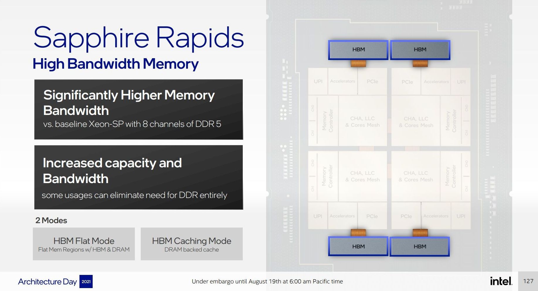
The other angle to Sapphire Rapids is the versions with HBM on board. Intel announced this back in June, but there haven’t been many details. As part of Architecture Day, Intel stated that that HBM versions of Sapphire Rapids would be made public, and be made socket compatible with standard Sapphire Rapids. The first customer of the HBM versions of SPR is the Argonne National Lab, as part of its Aurora Exascale supercomputer.
This diagram it showcases four HBM connections, one to each compute tile. Looking at the package, however, I don’t think that there’s realistically enough space unless Intel has commissioned some novel HBM that is long and narrow as it is in the diagram.
Even though Intel said that the HBM variants would be in the same socket, even their own slide from Hot Chips says different.
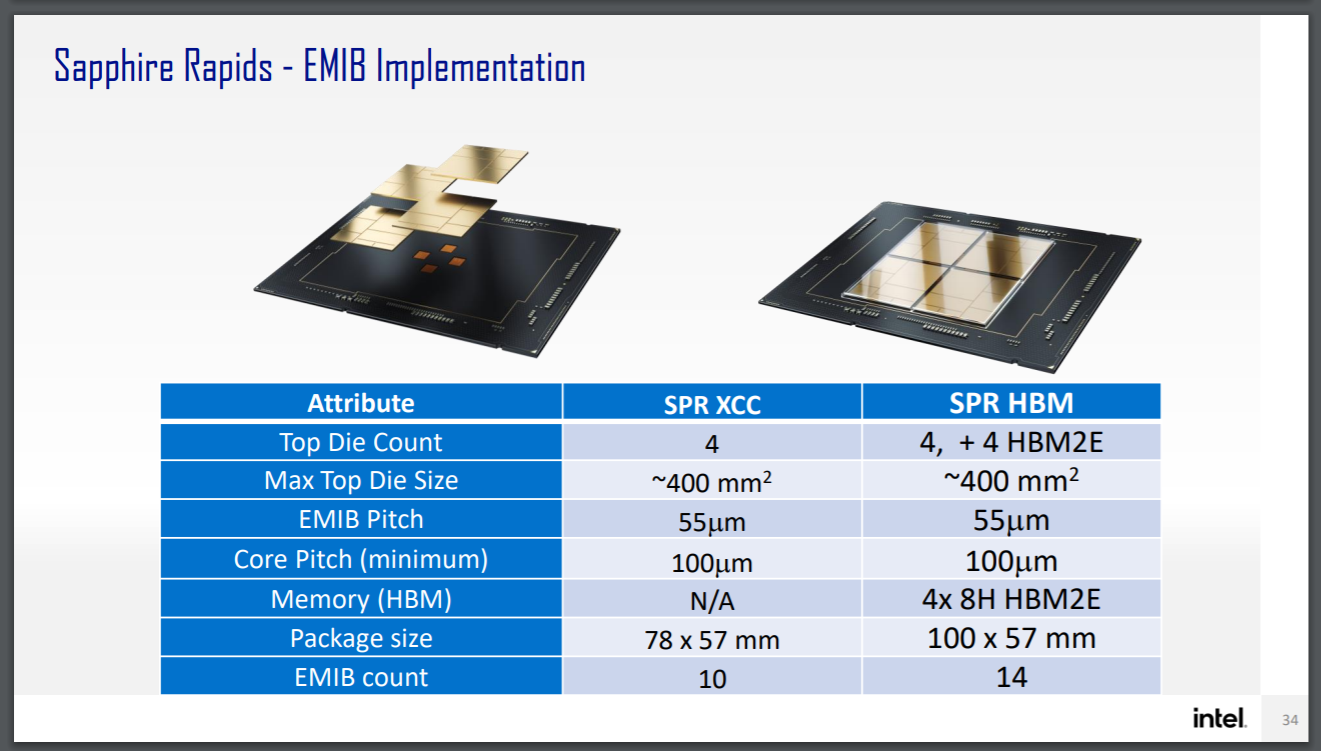
Here the package size with HBM says 100x57mm, compared to the SPR which is 78x57mm. So unless Intel is planning a reduced version for the 78x57mm socket, it's going to be in a different socket.
It is important to note that HBM will act in a similar capacity to Optane – either as an HBM flat mode with DRAM that equates the two, or as an HBM caching mode that acts similar to an L4 cache before hitting main memory. Optane on top of this can also be in a flat mode, a caching mode, or as a separate storage volume.
HBM will add power consumption to the package, which means we’re unlikely to see the best CPU frequencies paired with HBM if it is up against the socket limit. Intel has not announced how many HBM stacks or what capacities will be used in SPR, however it has said that they will be underneath the heatspreader. If Intel are going for a non-standard HBM size, then it’s anyone’s guess what the capacity is. But we do know that it will be connected to the tiles via EMIB.
A side note on Optane DC Persistent Memory – Sapphire Rapids will support a new 300 series Optane design. We asked Intel if this was the 200-series but using a DDR5 controller, and were told that no, this is actually a new design. More details to follow.
UPI Links
Each Sapphire Rapids Processor will have up to four x24 UPI 2.0 links to connect to other processors in a multi-socket design. With SPR, Intel is aiming for up to eight socket platforms, and in order to increase bandwidth has upgraded from three links in ICL to four (CLX had 2x3, technically), and moved to a UPI 2.0 design. Intel would not expand more on what this means, however they will have a new eight-socket UPI topology.
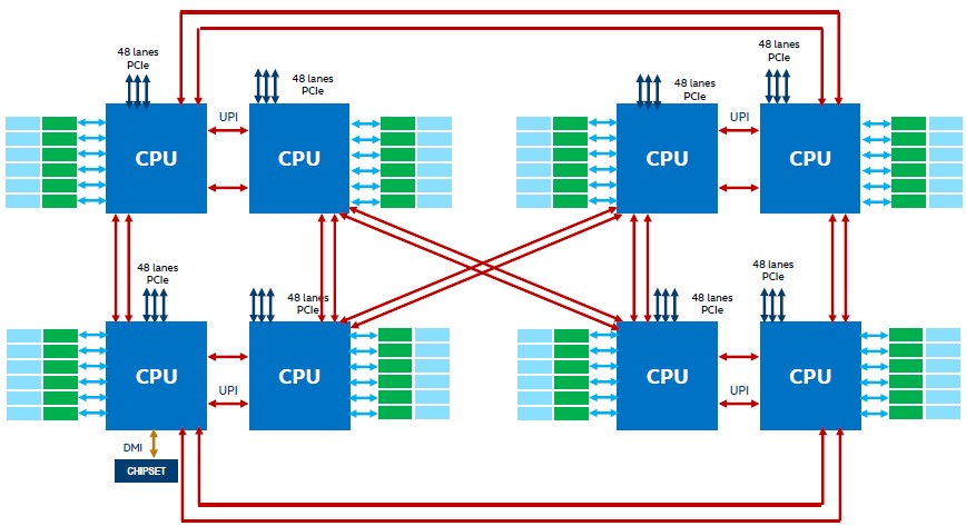
Current Intel Hypercube
Current eight-socket designs use a twisted hypercube topology: two groups of four form a box, and one pair is connected to the same vertex on the other set of four, while the second pair is inverted. Make sense? No, not really. Essentially each CPU is directly connected to three others, and the other four are two hops away. With the new topology, each CPU gets a direct connection to another, which moves the design more towards a fully connected topology, however exactly which CPU that connection should go to, Intel hasn’t stated yet.
Security
Intel has stated that it will be announcing full Security updates for SPR at a later time, however features like MKTME and SGX are key priorities.
Conclusions
For me, the improved cores, upgraded PCIe/DDR, and the ‘appears as a monolith’ approach are the highlights to date. However, there are some very obvious questions still to be answered – core counts, power consumption, how lower core counts would work (even suggestions that the LCC version is actually monolithic), and what the HBM enabled versions will look like. The HBM versions, with the added EMIB, are going to cost a good amount, which isn’t great at a time when AMD’s pricing structure is very competitive.
It is expected that when Sapphire Rapids is released, AMD will still be in the market with Milan (or as some are postulating, 3D V-Cache versions of Milan, but nothing is confirmed) and it won’t be until the end of 2022 when AMD launches Zen 4. If Intel can execute and bring SPR into the market, it will have a small time advantage in which to woo potential customers. Ice Lake is being sold on its specific accelerator advantages, rather than raw core performance, and we will have to wait and see if Sapphire Rapids can bring more to the table.
Intel moving to a tile/chiplet strategy in the enterprise has been expected for a number of years – at least on this side of the fence, ever since AMD made it work and scale beyond standard silicon limits, regardless of whatever horse-based binding agent is used between the silicon, Intel would have to go down this route. It has been delayed, mostly due to manufacturing but also optimizing things like EMIB which also takes time. EMIB as a technology is really impressive, but the more chips and bridges you put together, even if you have a 99% success rate, that cuts into yield. But that's what Intel has been working on, and for the enterprise market, Sapphire Rapids is the first step.


94 Comments
View All Comments
Silver5urfer - Tuesday, August 31, 2021 - link
Finally something innovative from Intel after years of abandonment of HEDT and Xeon leadership. I would give credit to Intel here because no big little BS scam. Mirroring the die mask design and using separate on top of the design which is using an EMIB on such a large silicon damn it looks super complicated vs AMD chiplet strategy.Now for the worst part, the I/O controller and Memory controller. That is going to be an issue for this design, Intel's mesh had power problems and inferior x86 performance on SKL Xeon and the Ice Lake solved that issue but core problem is AMD solved the EPYC 7000 series Zen based chiplets into a central I/O die and memory controller design eliminating the NUMA node performance hit. With smaller path trace due to EMIB this looks great but still it will have that hopping issues of Zen design based processors.
So a SPR based HEDT LGA4xxx socket is coming but when ? 2022 ? Zen 3 Threadripper Chagall / Genesis Peak is coming this year. And Zen 3 based V-Cache Milan EPYC will be coming next year once the factories start producing them and they will be dripped to AM4 socket processors. SPR needs to prove a lot, Zen 4 is dropping soon with 96C and beastly IPC on top of 12 Channel memory design on TSMC 5N.
IPC is a whole big another equation BUT most important is how the Intel 7 / 10nm design is vs TSMC 7N based EPYC in terms of clock potential and efficiency to performance ratios. Esp the fact that Intel had to cut off the x86 cores into those small SKL inferior crap cores onto the LGA1700 socket to keep up with the rising power consumption of their x86 processor designs. This one maxes out at 56C apparently with each tile at 14C, a big shame all these 14C couldn't make it to the LGA1700 they would have been perfect for the desktop compute, for those stupid thin and light BGA junk sales they axed it and shoved those efficiency designs into the Desktop LGA platform.
Kamen Rider Blade - Tuesday, August 31, 2021 - link
The NUMA Domain is going to be interesting with the 4x Memory Controllers split on each die having to cross domain boundaries.And there appears to be 2x Cross-Tile interconnects on each tile that hold CHA (Caching and Home Agent) and a LLC (Last Level Cache) to handle resolution of coherency across multiple processors.
Each core has a tiny CHA to check against the larger dedicated CHA & LLC to improve scalability according to the number of cores, memory controllers, or the sub-NUMA clustering mode. The address space is interleaved across different CHAs, which act like a single logical agent.
So that's a interesting solution to their data locality issues when multi-threading or having cross core communication.
repoman27 - Tuesday, August 31, 2021 - link
Why do you presume there will be any NUMA domain boundaries on-package? The whole point of going with EMIB and tiles vs. conventional chiplets on an organic substrate is that the EMIBs essentially act as "long wires" bridging the metal layers of the individual dies and extending the mesh without having to pipe the data over a separate link with a SerDes / PHY at each end.JayNor - Tuesday, August 31, 2021 - link
The leaked Emerald Rapids slides show CXL.mem. With the info that Sapphire Rapids doesn't implement CXL.mem, that finally makes sense.CXL.mem isn't mandatory according to servethehome article, "Compute Express Link or CXL What it is and Examples", from May 21,2021
JayNor - Tuesday, August 31, 2021 - link
The CXL.mem feature in Emerald Rapids can be seen in the slides in the adoredtv transcription article, "intel-rapidly-getting-worse", from June 29, 2021.Wereweeb - Tuesday, August 31, 2021 - link
Not what I wanted to see, but EMIB is a pretty cool piece of techBlastdoor - Wednesday, September 1, 2021 - link
Itanium, Optane, Knight's Landing, and Intel's original 10nm plans were all cool pieces of tech, too. Yet they lost to less cool tech like AMD64, flash, GPUs, and TSMC 7nm.After reading all this I'm left wondering if Intel designed this thing to showcase how cool EMIB is rather than EMIB enabling the optimal design (aka, a misalignment between cart and horse).
I look forward to seeing how this super cool glue compares to the combo of AMD"s Elmer's plus a big slab of SRAM plus high yielding multi-use chiplets.
Let's also see how yields and watts look.
wira6444 - Tuesday, August 31, 2021 - link
I though Intel hate "GLUE" ?Kamen Rider Blade - Tuesday, August 31, 2021 - link
They changed their mind.Oxford Guy - Thursday, September 2, 2021 - link
'Truth as convenience' is one of the defining qualities of corporate reasoning.