Arm Announces Neoverse V1, N2 Platforms & CPUs, CMN-700 Mesh: More Performance, More Cores, More Flexibility
by Andrei Frumusanu on April 27, 2021 9:00 AM EST- Posted in
- CPUs
- Arm
- Servers
- Infrastructure
- Neoverse N1
- Neoverse V1
- Neoverse N2
- CMN-700
Eventual Design Performance Projections
Alongside the ISO-process node IPC, power and area projections, Arm also made projection of possible eventual implementations of the V1 and N2. These would naturally no longer be ISO-process, but the company’s expectations of what actual possible products might end up as in future designs.
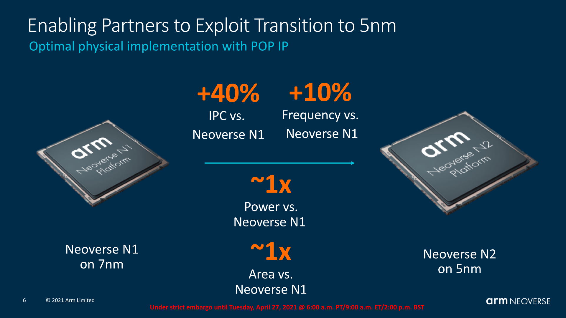
The most important slide and disclosure in this regard is the fact that a Neoverse N2 design on TSMC’s 5nm is expected to achieve the same power as well as the same area as a TSMC 7nm Neoverse N1 design today.
In general, that’s a relatively large presumption, but could possibly pan out if the vendors are able to achieve a good implementation. We don’t have too many details as to the 7nm node generation of Amazon’s or Ampere’s current N1 chips, but I would assume that they’re baseline N7 – at least similar to that of what AMD uses in their EPYC 7002 and 7003 chips.
Still, a -40% power reduction from N7 to N5 is a very high goal and assumption to make. The only N5 chips we’ve had in-house to date, the Kirin 9000, and Apple A14, showcased only a rough 10% efficiency advantage over their N7P predecessors. N7P being roughly 15% better than N7, that’s still only somewhat 26% better efficiency.
Arm expects that the current generation N1 implementations to day to not have fully achieved their potential as it was the vendor’s first attempt with the IP. Arm expects that the following generations with more experience, better implementations with for example more metal layers, to be able to squeeze out more performance and power efficiency on the N5 node.
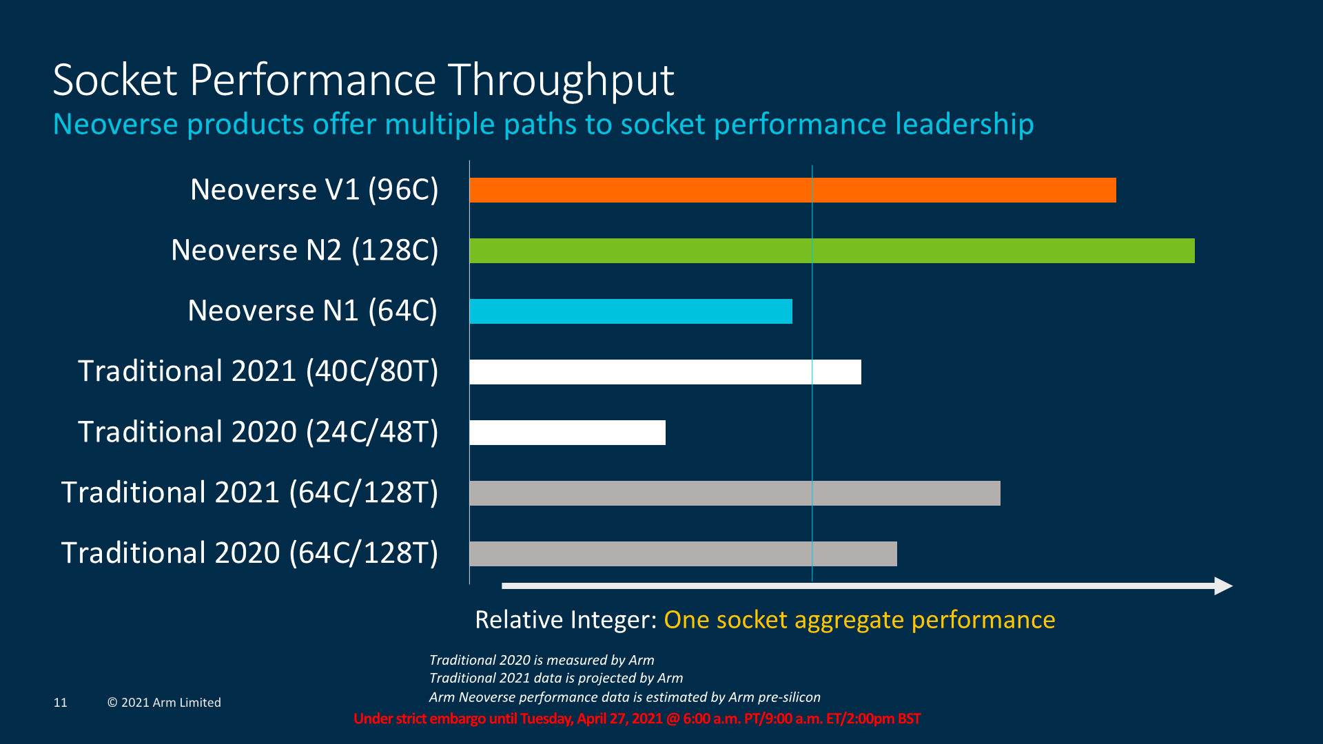
In terms of socket performance, Arm is expecting some very large generational gains versus a 64C N1 product today – it’s to be noted that these are Arm pre-silicon figures and not the Graviton2.
The “Traditional 2020” chips are the 24C Xeon 8268 and the 64C EPYC 7742. I would ignore the “Traditional 2021” parts here – Arm was aiming and estimating the performance of Intel’s newest 40C Ice-Lake and 64C Milan, however the presentation and figures here were integrated before AMD and Intel actually launched those systems – we have actual benchmark numbers in a custom graph below.
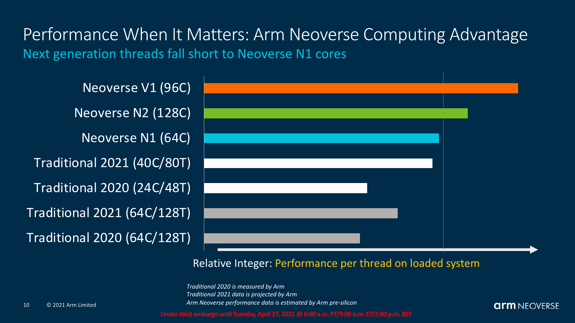
One metric Arm was focusing on was per-thread performance, where the “traditional” cores from AMD and Intel are falling short of the performance of Arm’s Neoverse cores.
Arm here is being somewhat sneaky in their presentation as they are trying to only focus on per-thread performance in cloud environments, where typically things operate on a vCPU basis, and essentially SMT-enabled designs from AMD and Intel naturally fall behind quite a lot in per-thread performance.
I can’t really blame Arm for depicting the performance figures like this – the cloud vendors today don’t really differentiate between real cores and SMT cores in vCPU environments, even having pricing that’s arguably unfair to SMT-enabled designs, which is why we’ve deemed Amazon’s Graviton2 m6g instances to vastly outperform AMD and Intel instances in terms of perf/W and perf/thread.

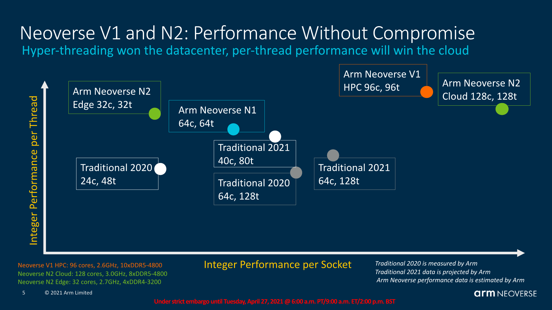
I wasn’t happy with Arm’s slides not including 1 thread per core performance figures for the SMT systems, so I included my own chart based on actual measured performance figures on the various platforms. The V1 and N2 figures use Arm’s performance scaling versus the Neoverse N1 datapoint, and I’ve baselined that to the Graviton2 scores we’ve measured earlier last year. Arm uses the same compiler flags as we do and also GCC 10.2, so the scores should also be compatible – with the only discrepancy being that Arm used 2MB page sizes.
The Neoverse V1 system uses 96 cores at 2.7GHz with 1MB L2 per core, on a 128MB 2GHz mesh, with 8 DDR5-4800 memory controllers. The N2 datapoint uses 128 3GHz cores at 1MB per L2, 96MB 2GHz mesh, with 10 DDR5-4800 memory controllers.
Arm’s per-thread performance lead doesn’t look that great here when looking at the 1T/C figures of AMD and Intel, but admittedly when in a vCPU scenario, Arm’s design would vastly outperform the SMT chips.
Generally speaking, the performance figures look good when it comes to per-socket performance, but generally that’s to be expected given the new 5nm process node and the more advanced memory controller technology in the projected figures.
AMD's next-generation Genoa should feature more massive performance jumps through the adoption of N5, DDR5, and transition away from their 14nm IO die. IPC and core count increases should also close the gap that’s depicted today. Intel’s next generation Sapphire Rapids should also improve the situation – albeit how that ends up depends on how much they’ll be able to squeeze out of 10nm SuperFin node in relation to what we’ve seen a few weeks ago on Ice Lake-SP.
Usually, I’m more open to Arm’s performance projections, however this time around the V1 and N2’s performance projections are extremely optimistic, especially since they’re completely dependent on the vendors achieving good implementations on N5 and actually reaching the projected 40% perf/W process node and implementation power efficiency gains. Based on what I’ve seen in the mobile space, I remain quite sceptical, and will be adopting a wait & see approach this time around.


95 Comments
View All Comments
name99 - Thursday, April 29, 2021 - link
What do you mean by "compare?"Apple is 8-wide Decode, Map, Rename. But that doesn't include the fact that Apple does a ton of clever work in those three stages (
- simple branches handled at Decode,
- a variety of zero-cycle moves and immediate handling in Rename
- two-level scheduler, with the higher level able to accept an 8-wide feed from Rename, even though the lower-level scheduler is narrower [6 for int, 4 for FP or LS] )
Apple is *astonishingly* wide at the completion end. 16-wide register freeing and history file release, up to 56(!!!)-wide release of ROB entries.
The Apple pattern so far (insofar as pattern-detection is worth anything) has been a 1st generation of four cores (A7/8/9/10) with similar design and 6-wide, constantly iterating on details within that framework;
then a 2nd generation (A11/12/13/14) that makes explicit the big.LITTLE structure (in A10 that was mostly invisible) and based on an 8-wide (with 6 integer units) structure.
If one has to bet, the reasonable thing to bet might be something like starting with A15 we transition to 10-wide (initially with6 later with 8 integer units), and 2xSVE256. Once again lay the framework, then scale out the pieces over the subsequent three cores.
One thing that is very clear (and presumably part of Apple's success) is that they have been very willing to keep modifying how they do things; they don't just settle on a design and leave it unchanged except perhaps for some scaling up. For example the way they handle the MOV xn, xm instruction has gone through at least three very different schemes. This may seem trivial (who cares about how a singe instruction is implemented?) except that these schemes indicate a substantial reworking of the entire register file and how registers are allocated and then freed.
This is in comparison to x86 which seems to live in (probably justified) terror that any change they make, no matter how low level, will probably break something because the whole system is so complex and so interconnected that no one person holds the entire thing in their head.
They also seem to have a good system in place for hiding new functionality behind chicken bits, so that they can effectively debug new features within shipping hardware. For example there are reasons to believe that A14 might have in place most of the pieces required for physical register file amplification (avoid allocation for back-to-back register usage and grab the intermediary off the bypass bus; early release of logically overwritten registers) but these are not visible -- probably behind chicken bits so that they can be tested under all circumstances in shipping HW, and made visible for A15.
And anyone who has not looked at the details is unaware of just how impressive the underlying Apple µArch platform is. There is substantial room there on-going growth! As I continue to explore it, not only do I see how well it works today, I also see multiple directions in which it could "easily" (ie feasibly, on schedule and within budget) be improved for years to come. The only other artifact I know of that comes close in terms of quality of implementation and ability for continuing growth is the Mathematica code base -- other artifacts like other CPUs, or various OS implementations, are in a totally different (and far inferior) league.
name99 - Thursday, April 29, 2021 - link
To expand on my point, it's great that ARM are including so many good idea, but it's also astonishing the extent to which pretty much every good idea already has an Apple precedent.For example consider the MPAM discussion: "The mechanism to which this can be achieved can also include microarchitectural features such as dispatch throttling where the core slows down the dispatched instructions, smoothing out high power requirements in workloads having high execution periods, particularly important now with the new wider 2x256b SVE pipelines for example."
This sounds like (and IS) a good idea -- certainly a lot better than reducing frequency the way Intel does for AVX512.
But look at this Apple patent from 2011(!)
https://patents.google.com/patent/US9009451B2
"A system and method for reducing power consumption through issue throttling of selected problematic instructions. A power throttle unit within a processor maintains instruction issue counts for associated instruction types. The instruction types may be a subset of supported instruction types executed by an execution core within the processor. The instruction types may be chosen based on high power consumption estimates for processing instructions of these types. The power throttle unit may determine a given instruction issue count exceeds a given threshold. In response, the power throttle unit may select given instruction types to limit a respective issue rate. The power throttle unit may choose an issue rate for each one of the selected given instruction types and limit an associated issue rate to a chosen issue rate. The selection of given instruction types and associated issue rate limits is programmable."
I just keep bumping into this stuff! Arm release new cores with what seem like good ideas (and of course ARM tell us a lot more about what's new than Apple does). I do some exploring -- and find Apple patented that idea five or more years earlier!
mode_13h - Thursday, April 29, 2021 - link
> consider the MPAM discussionThe slide calls that MPMM. The article confuses it with Memory Partitioning And Monitoring.
Anyway, the N2's PDP sounds a lot more advanced.
GeoffreyA - Friday, April 30, 2021 - link
Zen 3 needn't blush when standing next to Apple. 4-wide decode might be small but that does pick up to 6, coming out of the micro-op dispatch. Then, going down, you've got 10-wide issue on the INT side, and 6-wide on FP. Admittedly, narrower register files and 8-wide retire from the (smaller) ROB, along with smaller caches. As for move elimination, even Skylake has that. Yes, everything tends to be narrower. But I think it goes to show there's nothing particularly out of this world on the Apple side.name99 - Friday, April 30, 2021 - link
I did not say that move elimination was the interesting part.I said that what was interesting is that over Apple's short CPU career they have already implemented it in three significantly different ways.
That strikes me as interesting and important -- there is no resting on the laurels, no acceptance that "we have the feature, OK to slow down". You honestly believe that Intel operates according to that same mentality?
GeoffreyA - Friday, April 30, 2021 - link
I'll admit, Apple isn't resting; and they aren't scared to break orthodoxy in advancing their designs. If the others do not wake up, they'll be left in the dust. As for Intel, complacency has put them in the well-deserved pickle they're in today. AMD deserves credit, though, for doing much these past few years; and, like Apple, aren't resting on their laurels either (arguably like they did in the K8 era).mode_13h - Friday, April 30, 2021 - link
How big are Apple's cores, though? Area is tricky, because they tend to be on a newer process node.But, my point is that maybe AMD and Intel aren't making their cores even larger and more complex, because they're targeting the server market and found that a more area-efficient way to scale performance is by adding more cores, rather than making their existing cores even more complex.
name99 - Friday, April 30, 2021 - link
A14 is 88mm^2.Eyeballing it, each large core is about 2.5% of that area, so 2.2mm^2
Throw in the L2 at about 3.5%, so 3mm^2 (shared between two cores).
Throw in the SLC (not exactly an L3, but pretend it is if you insist) at 8.8% and about 8mm^2.
I guess if you were targeting a server type design, we could probably treat it as something like
2.5+(3/4)+ (8.8/8) [making rough guesses about what sort of L2 and L3 would be optimal for a server type design] so ~4.4mm^2.
Could fit ~100 in a 440mm^2 (though you'd also want some memory controllers and IO!)
Definitely a lot larger than something like an N1 or N2 -- but of course, Apple isn't designing for the data center -- if they were, they'd probably adopt something halfway between Fire Storm and Ice Storm.
The problem is not that Intel and AMD are chasing the server market, it is that the way they are chasing it is incoherent. IF your primary goal is the server market, then WTF are you designing for super-high frequencies? The data center cores never run at those frequencies -- but being able to boast about them means your transistor density is half to a third that of Apple (or more relevant ARM/Altra/Graviton) on the same process...
Pick a goal and optimize for it! But Intel's goal seems to be to optimize for marketing that they can hit 5.x GHz (for half a second...) Not clear that designing the entire company around that goal (of zero interest to the data center, and little interest to most users) is such a great long-term strategy.
mode_13h - Saturday, May 1, 2021 - link
> IF your primary goal is the server market, then WTF are you designing for super-high frequencies?AMD actually has lagged Intel in frequency, and I think that's one of the reasons. Remember, AMD is the only one using the same exact silicon on both the mainstream desktop and in all their server products.
Intel, on the other hand, has completely separate silicon for their server dies, and we don't know all of the subtle ways they could differ from their desktop or laptop cores. We just know they tend to reuse the same basic core micro-architecture up and down their product lines (except for the really cheap/low-power stuff).
> The data center cores never run at those frequencies
A few Cascade Lake Xeons could turbo up to 4.5 GHz, which benefits certain workloads. The fastest turbo clock of an Ice Lake Xeon is 4.4 GHz
The fastest EPYC can boost up to 4.1 GHz.
In Intel & AMD's defense, a simpler core can clock higher, but runs more efficiently at lower clocks and enables higher densities. So, it seems like a pretty good strategy to me.
> Pick a goal and optimize for it!
Like ARM, Intel and AMD trying to balance power (in a server/laptop application, at least) and area. Apple is the only one who really has the luxury not to care much about area and just optimize for a single target. When Apple reuses its laptop core micro-architecture in both desktops AND servers, then we can compare them to the other guys. Until then, I think it's a case of Apples and pears.
GeoffreyA - Saturday, May 1, 2021 - link
"Until then, I think it's a case of Apples and pears."I think that's it. Well, soon process improvements will be a thing of the past, owing to quantum effects, and then we'll see who does what. The free ride is almost over.