Qualcomm Details The Snapdragon 888: 3rd Gen 5G & Cortex-X1 on 5nm
by Andrei Frumusanu on December 2, 2020 10:00 AM EST- Posted in
- Mobile
- Qualcomm
- Smartphones
- SoCs
- 5G
- Cortex A78
- Cortex X1
- Snapdragon 888
Triple ISPs: Concurrent Triple-Camera Usage
Interestingly enough, during yesterday’s keynote event, Qualcomm described themselves as a camera company, which is a funny way to see things, but actually somewhat makes sense given the large leaps in smartphone camera capture capabilities over the recent years.
The new Snapdragon 888 pushes the envelope in terms camera abilities by adding a whole new independent third ISP to the SoC, allowing the SoC to now run three independent camera modules concurrently, opening up new use cases for vendors and camera applications.

The new triple-ISP architecture now increases the overall pixel processing throughput by 35% to 2.7Gigapixels/s, allowing for concurrent usage of up to three 28MP sensors with zero shutter lag captures. Alternatively, you can use a combination of 64+25MP sensors with ZSL, or a single 84MP sensor with ZSL. There’s still also support for ultra-high-resolution sensors up to 200MP, but image captures here don’t support ZSL.
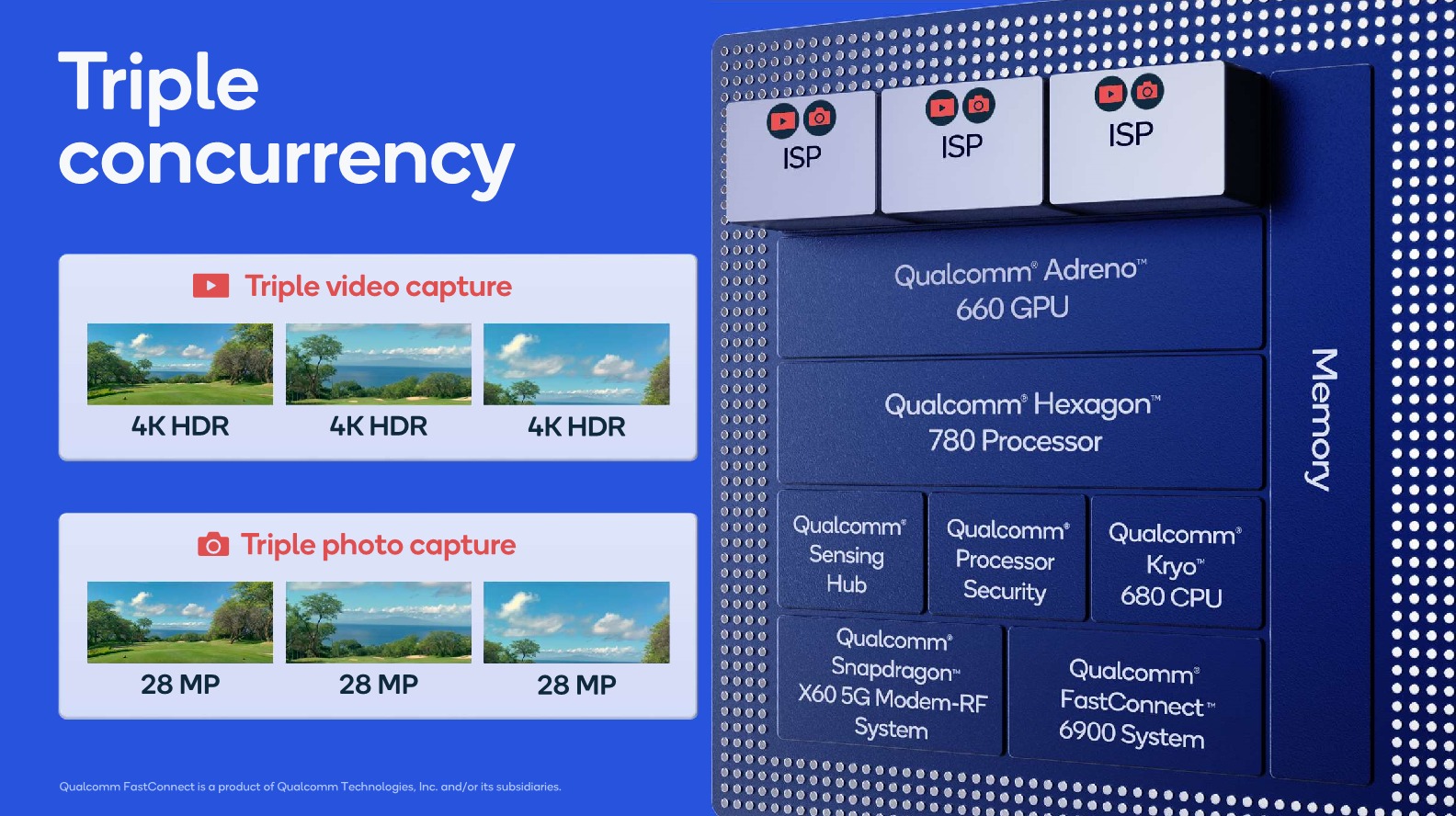
Allowing concurrent captures of three sensors now allows for the holy trifecta of ultra-wide-angle, wide-angle and telephoto modules to capture a scene at the same time, allowing for more interesting use-cases such as image stitching and image fusion to happen to seamlessly.
One interesting capability that Qualcomm was advertising is triple-stream 4K HDR video recording. That’s a bit of an odd-ball use-case as I do wonder about the practical benefits, but I do at least hope that the new triple ISP system allows for more seamless switching and zooming in and out between the various camera modules during video recording.
Video recording capabilities this year don’t seem to have changed, compared to the Snapdragon 865. This means 4K120 or 8K30 are still the peak capture modes, supporting also slow-motion of 720p960. Formats are also unchanged, with HEVC encoding in HDR formats such as HDR10+ or Dolby Vision being supported.
AV1 decoding didn’t make the cut this year unfortunately, which means wide-spread adoption in mobile for the codec will be delayed for another year.
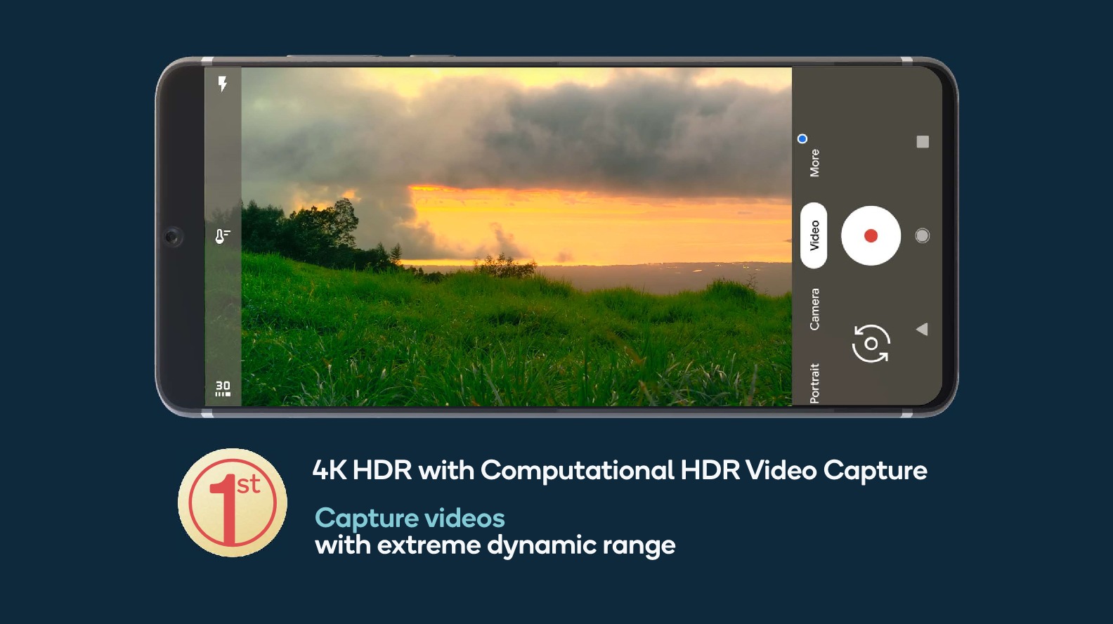
While the video encoding formats haven’t changed, the image processing capabilities for HDR capture has. Thanks to the new ISPs and the raw performance throughput, the new Snapdragon 888 will be able to capture 4K HDR footage with the more advanced computational HDR processing being applied on each and every frame of the video.
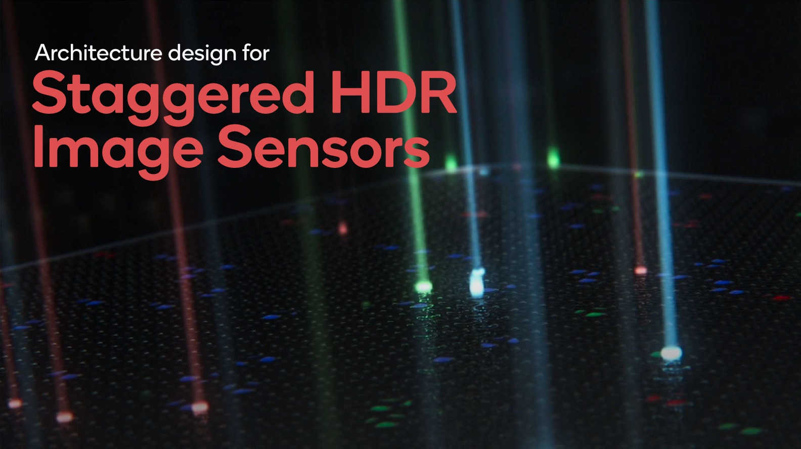
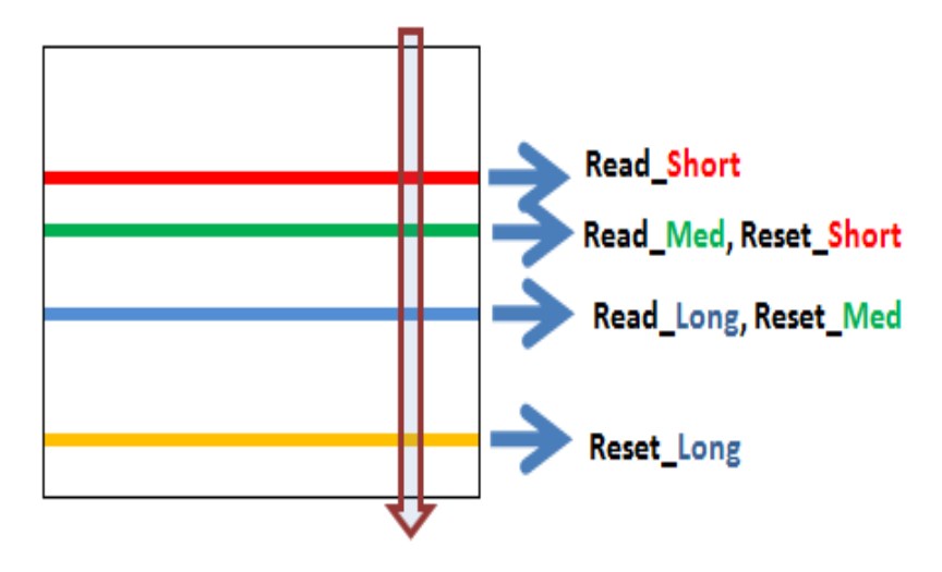
Qualcomm claims that the new ISP in the Snapdragon 888 is the first to support new next-generation staggered HDR sensors.
Source: OmniVision
These are sensors that can have multiple rolling shutters, meaning sensor line readouts, active at the same time on the sensor. Instead of taking multiple exposures one at a time sequentially by scanning out the sensor matrix from start to finish, the sensor will start another exposure immediately after the completed line read-out, reducing the time in-between exposures greatly. This should allow for significant less motion ghosting between the exposures and a sharper resulting recombined HDR image capture than current generation sensors which only have a single active line readout on the sensor.
While we haven’t actually heard of such sensors from Samsung or Sony yet, Qualcomm is adamant that we’ll be seeing smartphones in 2021 employing this new technology.

A further improvement for still-picture captures is the advancement of the new multi-frame noise reduction engines inside of the ISPs. It’s said that the quality of the noise reduction has been improved this generation, allowing for even better low-light captures with the native capture mode (no computational photography).


123 Comments
View All Comments
MenhirMike - Wednesday, December 2, 2020 - link
Apple bought P.A. Semi in 2008 to make their own ARM Chips, and evidently, P.A. Semi is a better semiconductor company than Samsung, Qualcomm, and anyone else in the ARM marketplace.Ppietra - Wednesday, December 2, 2020 - link
P.A. Semi no longer exists and a lot of things happened since P.A. Semi was bought, like Apple buying Intrinsity which was involved in the creation of the A4 chipjordanl17 - Thursday, December 3, 2020 - link
I remember the headline a long time ago.. "Apple buys Israeli based cpu developer to make their own chips" I was like, "haha, yeah, good luck what that" I. WAS. WRONG.jordanl17 - Thursday, December 3, 2020 - link
maybe they weren't Israeli based... (can't edit post?)Luminar - Thursday, December 3, 2020 - link
The edit functionality only exists for the first 15 seconds after posting. This is to prevent people from going back and editing their comments well after the fact to appear less wrong.Wilco1 - Friday, December 4, 2020 - link
This is not true - if it was, I could edit this!trini00 - Saturday, December 5, 2020 - link
https://www.zdnet.com/article/start-up-plans-new-e...Quite a interesting read, integration on a chip and the cache structure is some of the advantages M1 has.
headeffects - Wednesday, December 2, 2020 - link
Is this true? I knew Samsung’s 5nm was behind but behind even the TSMC 7nm sounds shocking.Lodix - Thursday, December 3, 2020 - link
NoPpietra - Wednesday, December 2, 2020 - link
I am no expert but I believe it happened because of very different visions/philosophies and objectives.ARM goes for smaller and less complex cores than Apple, believing it will consume less and that this will save space so it can add more cores in the same die, hoping for higher multithreaded performance. This would also probably be cheaper for other companies to implement.
Apple on the other hand bet on bigger cores, maybe already envisioning that its development could in the end be more useful for computers, or at least the iPad. Apple believed that a faster core could consume less by finishing more complex tasks sooner. Costs didn’t seem to be a big concern for Apple, nor increasing the core numbers like crazy (remember when there were SoCs with 10 or more cores in phones?), nor Apple was constrained by what others might need. I imagine with these objectives Apple had to solve a lot of problems to optimize power consumption. Having to go through these challenges much sooner than ARM probably helped Apple to develop more efficient designs.
It seems that Apple is just far more aggressive in developing its chips, and knows what it needs for its hardware and software.