Qualcomm Details The Snapdragon 888: 3rd Gen 5G & Cortex-X1 on 5nm
by Andrei Frumusanu on December 2, 2020 10:00 AM EST- Posted in
- Mobile
- Qualcomm
- Smartphones
- SoCs
- 5G
- Cortex A78
- Cortex X1
- Snapdragon 888
Conclusion & First Impressions
The new Snapdragon 888 is overall a very impressive package from Qualcomm, advancing the most important areas for which today’s smartphones are being used. 5G connectivity was the big new feature of 2020 SoCs and smartphones, and the new 888 platform represents the evolution and maturing of the new technologies that had been introduced in prior generations.
The big focus point of the Snapdragon 888 were clearly AI and cameras. The new Hexagon 780 IP block looks immensely impressive and to me seems like a major competitive advantage of the new SoC design – other vendors which aren’t as vertically integrated with their accelerator IPs will have to respond to Qualcomm’s new advancements as it seems like a major performance advantage that will be hard to mimic.
Today’s flagship smartphones have diminished ways of differentiating themselves from one another, with the cameras still being the one aspect where vendors still have very different approaches to their designs. Qualcomm’s push for a triple-ISP system in the Snapdragon 888 pushes the upper limits of what vendors will be able to do on their smartphones, allowing for a continued push for the smartphone camera ecosystem. Even for still-picture camera experiences, it seems that Qualcomm is expecting a more notable technology jump in 2021 as we see the introduction of new sensors and imaging techniques, enabled by the new SoC.
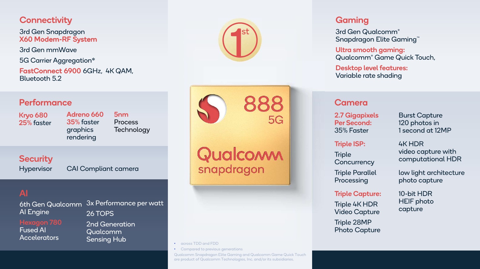
The new CPU configuration gives the new SoC a good uplift in performance, although it’s admittedly less of a jump than I had hoped for this generation of Cortex-X1 designs, and I do think Qualcomm won’t be able to retain the performance crown for this generation of Android-SoCs, with the performance gap against Apple’s SoCs also narrowing less than we had hoped for.
On the GPU side, the new 35% performance uplift is extremely impressive. If Qualcomm is really able to maintain similar power figures this generation, it should allow the Snapdragon 888 to retake the performance crown in mobile, and actually retain it for the majority of 2021.
The new Snapdragon 888 to me looks like a continuation of Qualcomm’s excellent execution over the last few years. Striking a balance between performance, power efficiency, and features is something that may be harder than it sounds, and Qualcomm’s engineering teams here seem to be focused on being able to deliver the overall best package.
Much like the Snapdragon 865, and the last couple of generations of Snapdragon SoCs before it, I expect the new Snapdragon 888 to be an excellent foundation for 2021’s flagship devices, and I’m looking forward to experience the new generation.
Related Reading:
- Qualcomm Tech Summit 2020: Day One LiveBlog (10:00 ET, 15:00 UTC)
- Qualcomm’s New 3rd Generation Snapdragon X60 5G Modem, Built on 5nm
- Qualcomm Announces Snapdragon 865+: Breaking the 3GHz Threshold
- The Snapdragon 865 Performance Preview: Setting the Stage for Flagship Android 2020
- Qualcomm Announces Snapdragon 865 and 765(G): 5G For All in 2020, All The Details
- The Snapdragon 855 Performance Preview: Setting the Stage for Flagship Android 2019
- The Qualcomm Snapdragon 855 Pre-Dive: Going Into Detail on 2019's Flagship Android SoC


123 Comments
View All Comments
eastcoast_pete - Wednesday, December 2, 2020 - link
Thanks Andrei! While not the or even a focus of your article (there was no need), I am struck by how stuck ARM bigLittle type designs are when it comes to the efficiency cores. A55, still? Let's make no mistake, you/we want capable and efficient small cores in the SoC, so that the big cores don't feast on the battery all the time. 5G modems tend to increase power use (this integrated one hopefully a bit less), so having the ability to stay on the low power cores of the CPU longer is even more important.Andrei, if you can, I'd appreciate a deeper dive into the state of the art of the small cores, especially a comparison of Apple's vs. stock ARM A55 designs. Thanks!
psychobriggsy - Wednesday, December 2, 2020 - link
I imagine that there's only so far you can take an in-order ARMv8 core design when you want to optimise for power consumption. ARM do release updates to their core designs, whilst retaining the same name as well, so they do get small improvements. There are no ISA changes for these consumer cores either, as far as I am aware.But it does look like the A55 has pretty much not changed much in several years, and simply become more and more efficient as the process has shrunk down to 5nm and the clocks have remained the same. I think people were expecting an A58 by now - maybe there will be an A59 to go with the A79 next year?
Lolimaster - Thursday, December 10, 2020 - link
Probably called A63.Ppietra - Wednesday, December 2, 2020 - link
This is what he said about the icestorm cores in the A14:"The performance showcased here roughly matches a 2.2GHz Cortex-A76 which is essentially 4x faster than the performance of any other mobile SoC today which relies on Cortex-A55 cores, all while using roughly the same amount of system power and having 3x the power efficiency."
brucethemoose - Wednesday, December 2, 2020 - link
Makes one wonder what on earth Apple is doing to achieve that. Its not like ARM's CPU architects are underpaid chumps.Some of it is extra die space, I guess? The LITTLE cores have to be, err, little, while Apple can afford to blow up area for efficiency.
tkSteveFOX - Wednesday, December 2, 2020 - link
Not really. Apple's chips are always roughly the same size as QC and Kirin top chips and on the same nodes.Just better architecture and more R&D investment. QC have been doing the same chip for 3 gens now, just updating the ARM tech and gains in AI and ISP, but the CPU config remains the same, it's even clocked the same!
Ppietra - Wednesday, December 2, 2020 - link
I think Apple CPU cores are significantly bigger than ARM designsheadeffects - Wednesday, December 2, 2020 - link
I don’t have all the numbers on me but Apple has never had an on die modem while Qualcomm usually does, so you can’t directly compare die sizes like that. Andrei would perhaps know the measurements of the actual core sizes and how they compare from Apple to Qualcomm.Fulljack - Thursday, December 3, 2020 - link
Nope. Apple A13 is 98,48 mm² while Snapdragon 865 is 83,54 mm²—according to TechInsights. Both are manufactured on TSMC N7P and feature no integrated modem. So yeah, wider (and thus bigger) cores design does improve performance, but not always though.RSAUser - Wednesday, December 2, 2020 - link
Apple has both an architecture design leas and a process node lead, TSMC 5nm vs Samsungs Marketing Version of it which is worse than TSMC 7nm.