What Products Use Intel 10nm? SuperFin and 10++ Demystified
by Dr. Ian Cutress on September 25, 2020 9:00 AM EST10nm Takes a Different Tack: Cannon Lake to Ice Lake
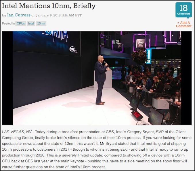
In Intel’s own words, it shipped its first 10nm products for revenue by the end of 2017. These first processors, known as Cannon Lake, were shipped to a number of OEMs and stealthily hidden from the public, being pushed into commercial and educational products in China and others.
The processor had only two cores active, and the integrated graphics was broken, giving an indication of how well the first generation of 10nm was progressing. Intel had already committed to shipping 10nm for revenue by the end of 2017 to its investors, and the small side announcement at CES 2018 (it wasn’t mentioned in the keynote) followed by the small trickle of almost non-existent Cannon Lake product over 2018 technically fulfilled Intel’s obligation.
 Click through to see the video
This version of 10nm didn’t get off the ground. Intel eventually put it into the Crimson Canyon NUC family in late 2018, but it was slower than the 14+++ processors it was meant to replace, and used more power.
At the time when Intel announced 10nm was shipping for revenue, it had already announced that the next generation product was going to be called Ice Lake, built on ‘10nm+’. By Intel’s Architecture Day in December 2018, the company tried to quietly rebadge Ice Lake as 10nm – when asked about the change and if this version of 10nm was any different to Cannon Lake, Intel’s Raja Koduri, partnered with Murthy Renduchintala, stated that ‘[10nm] is changing, but it hasn’t changed’. If ever there was a cryptic answer, this was it.
Ice Lake Rebadged to 10nm: Why?
So now we have Cannon Lake on ‘10nm’, and Ice Lake originally on 10+ but now rebadged to 10nm, but a different 10nm, with no real explanation as to why. In discussing with a number of peers and analysts in private conversations, the apparent conclusion they have come to is that Intel did not want to admit that its first generation of 10nm product had failed. Ever since then, Intel has attempted to quietly and discreetly shift Cannon Lake under the rug, as if it didn’t exist (it does exist, we did a big review on it, and Crimson Canyon is still for sale today at some of Intel’s biggest partners and major retailers).
Without Intel needing to admit that the first generation had failed, Ice Lake was the true ‘native’ 10nm product that was destined for life in the fast lane for consumers. If that was the case, then the low key presentation at CES 2018 stating it was shipping in 2017 was simply to meet investor targets. Intel never promoted Ice Lake as its first 10nm product, but the fact that the Cannon Lake product wasn't great meant that the company had to try and remove it from people's minds.
On Ice Lake, we studied the Ice Lake design, and we’ve seen lots of notebooks built on it. The fact that Intel called it ‘10th Gen’, and then also released the Comet Lake 14++++ product also called ‘10th Gen’, really ended up confusing the company even more, even in presentations to the press. It was the first time Intel had two products within the same generation of marketing name under different process nodes. It even confused OEM partner marketing teams as well as sales staff.
The problem with calling Ice Lake the new 10nm, is that internally the engineers still called it 10+. As Intel also announced other new products, such as Snow Ridge, or Lakefield, despite these meant to be called under the new 10nm, they would often be cited as ‘10+’ depending on which department of Intel you spoke to.
10nm Takes a Different Tack: Sapphire Rapids and Tiger Lake
In later 2019, during Intel’s HPC DevCon event focusing on supercomputers, the company discussed its post-Ice Lake server processor, Sapphire Rapids. It had already been announced that Sapphire Rapids was to power the Aurora supercomputer (which was originally supposed to have a 10nm Xeon Phi processor), however as part of the DevCon event we were discussion Sapphire Rapids in the context of a 10+++ process node. This event was mostly under the auspices of engineers, and those engineers were using 10+++ under the oldest naming scheme to identify Sapphire Rapids, or in other conversations, 10++. We were subsequently corrected by marketing in confirming that the official process node name was 10++; the engineers somewhat scoffed at this as a knock on effect to the Ice Lake name changing.
With the confusion on what to call these products between marketing and engineering, the discussions between the two (at least, from my perspective) didn’t really have any teeth at the time. Engineers didn’t either know about the new naming scheme, or didn’t understand why marketing had changed the names. Marketing wasn’t always there to correct engineering when speaking externally, and even if they were, sometimes the engineers wouldn’t understand the reasons why the names had changed. It starting to come to a head when Intel was discussing the product after Ice Lake, called Tiger Lake.
At CES 2020, the company announced Tiger Lake to the world in its Keynote address. As part of that keynote, as well as the press briefings, there was a lot of discussion as to whether this was a 10++ or 10+ product. People were getting confused between the old naming schemes and the new naming scheme, and whichever one was being used at the time.

I have continually had the conversation, especially at technical events, where I need to ask someone from Intel to clarify which scheme they were working under for any given product. For anyone outside of this bubble trying to keep track of it all, I can’t imagine what headaches you might have had – I was talking directly to Intel a lot of the time and it was giving me plenty of headaches! As Intel started announcing more 10nm-class products from different portfolio lines, each business unit had its own engineers in its own state of confusion. This came to a head when Intel changed the naming a second time.
No More Pluses, It’s All About SuperFin
As part of Intel’s Architecture Day 2020, the company did three things:
- Go into detail about Tiger Lake
- Go into detail about DG1 Xe Graphics, and new products in the portfolio
- Rename the different 10nm process node using SuperFin
As part of that event, Intel went into some detail about its new ‘SuperFin’ technology. Using an updated metal stack and new capacitor technology, Intel had designated its latest BKM update for Tiger Lake and DG1 graphics as ‘10nm SuperFin’.
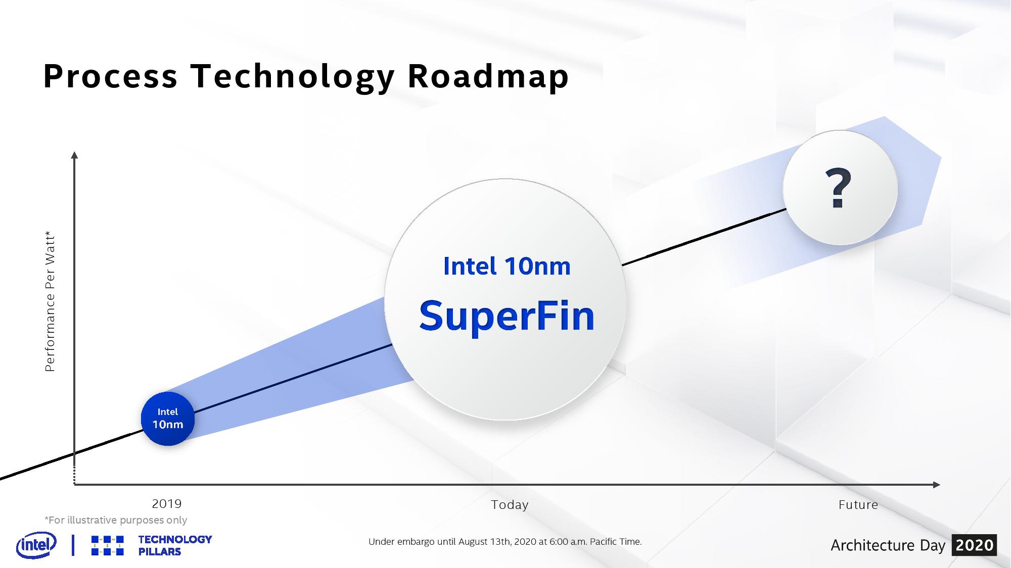
This is very much a marketing name, but the idea from the point of view of Intel’s communications team was to rebadge every 10nm product from Intel with some new variation of SuperFin as needed. This pushed Intel away from the ++++ nomenclature (something I’d advocated for anyway), and gave an opportunity for the company to realign all of its manufacturing branding with this new scheme.
While an interesting direction, Intel’s communications team has had two problems with this.
- Most/Some engineers were still working on the original naming scheme
- Some engineers/marketing were working on the first updated naming scheme and didn’t get the memo
Since changing from + and ++ to SuperFin, I have had a number of confusing calls with Intel’s engineers.
At Hot Chips in August, I was told by the presenter of the Ice Lake Xeon processors that the technology was an ‘enhanced 10nm’, which could have been meant as 10+, under the original naming scheme.
Even this week, for the launch of Intel’s new embedded Atom CPUs, I was told these CPUs were ‘10++’, without any indication of which naming scheme they were using. I was then told it was SuperFin. After the press release was changed for SuperFin, and we published our article, it was noticed that Intel's own product database had it listed as regular 10nm, no SuperFin. It turns out that it was regular 10nm, no SuperFin, the same as Ice Lake.
Even when directly discussing with Intel’s communication teams, they would start referring to the original naming scheme, or the first updated scheme. I've had to request double confirmation on multiple occasions. While Intel has a main HQ communications team, each business unit inside Intel has its own PR people. Each business unit may also be working with a PR agency (sometimes different to each other), and then beyond that, there may be different PR connections for each region, and then each with its own localized PR company. Renaming a product or a process is thus a very hard thing to force down every channel, compared to a new product which should have the right name on the initial documents.
When speaking with Intel’s lead Tiger Lake engineers in a 1-on-1 interview, I asked them outright if the new SuperFin naming scheme was being used by the engineering teams. I was told that for the most part, it was. I followed up asking if mistakes and slip ups were made, and the answer came back in the affirmative. It’s somewhat clear that the Engineering teams don’t like being pushed around by the marketing/communications teams in this way, having to change internal documents and naming processes in order to internalize what stuff is being called when it can’t be called what it originally was almost a decade ago. We see the same thing when engineers are rolled out to present about new products – they will call the processors by the internal code names, not ‘Core 10th Gen’ or similar, and often have to stop themselves by continually saying the code name.


143 Comments
View All Comments
lilo777 - Friday, September 25, 2020 - link
I totally agree. People obsessed with process names should check this article - https://hexus.net/tech/news/cpu/145645-intel-14nm-...It shows that transistor density of Intel 14nm+++ is close to that of AMD/TSMC 7nm.
Spunjji - Friday, September 25, 2020 - link
It really isn't when you compare the whole chip - they appear to have compared some of the worst structures for scaling in that article.Nobody's really obsessed with names - they just serve a useful purpose for discussing differences.
lilo777 - Friday, September 25, 2020 - link
They are not. After advent of finfet (and maybe even before it) process names do not carry any useful information about the merits of the process. It's just a name of the menu item in foundry's catalog. If they wanted to, Intel could name their next process 1nm. They won't. Nobody cares.Spunjji - Monday, September 28, 2020 - link
Process names stopped relating to most structure sizes way before FinFet, and I'm well aware that the name itself - on its own - doesn't convey useful information about the process. What they do convey is which process came after which for a given foundry, they imply significant difference such as a decrease in average feature size, and sometimes they convey a general idea of which industry generation the process belongs to. what they don't tell you is whose foundry produces smaller and/or more performant transistors, but as I said in the first place, they're useful as a simple reference point for discussion; you can't easily discuss something that doesn't have a name.Intel won't name their next generation 1nm because it wouldn't be the next logical step after their current generation. You're literally proving yourself wrong by pointing out that they won't do that.
You also totally skipped past copping to the falsehood that 14nm+++ is "close to" TSMC 7nm. 14nm++ is around 37.22 MTr/mm² (Source: https://en.wikichip.org/wiki/mtr-mm%C2%B2 ) while Renoir on 7nm measures in at about 63 MTr/mm².
FullmetalTitan - Saturday, September 26, 2020 - link
That TEM cut looks an awful lot like SRAM block, which has notoriously poor scaling with design node. SRAM cells from 28nm generations are not double the size of 14nm SRAM cells, more like 20% larger.However as you point out in your next comment, node naming stopped being a useful metric, somewhere between 65nm and 45nm. The industry stuck with it based on IEEE roadmap of full-node step naming, but it doesn't remotely align with the reality. The old standard was full width half pitch, since the center to center distance between gates was approximately aligned with the channel width. Intel led the industry departure from that standard, instead measuring the effective gate length. In later generations of planar nodes (45nm and smaller) gates were packed densely enough that FWHP was not accurately representing gate width anymore, it was SMALLER than the gate dimension. With FINFETs that actually went a bit far in the other direction since the control surface width of a fin is not the same as a planar device, since the gate wraps over the fin and the surface area is the important factor in design and operation. For the 14/16nm generation of devices, the minimum feature size of interest was actually 6-7nm for Intel, TSMC, and Samsung nodes.
Spunjji - Monday, September 28, 2020 - link
Yup, you nailed it on that one. False conclusion (similar density) drawn from incomplete information (only one type of transistor measured).RSAUser - Saturday, September 26, 2020 - link
These are all from "IC Knowledge LCC" as posted by electronics weekly.Transistor density (MTx/mm2)
Intel 10nm: 106
Samsung 5LPE: 133.56
TSMC 5FF: 185.46
Then from other places, this is Wikipedia, but following links to check that they're right:
TSMC N7FF (First generation 7nm): 96.5
So TSMC's first 7nm generation is nearly as dense as Intel's first 10nm, interesting. Meanwhile TSMC's N7FF+ is 114, Apple's A13 chip is built on this.
Their 5nm node is supposedly 186, it's used for Apple's A14 chip.
Spunjji - Monday, September 28, 2020 - link
That number for Intel 10nm isn't accurate - it was their original target and it hasn't been reached in practice. It looks like they had to relax a lot of their design rules to make the process yield well.Anandtech's quoted number for density with Lakefield is 49.4 MTr/mm², while apparently Tiger Lake is closer to 40 MTr/mm².
Bagheera - Tuesday, March 9, 2021 - link
you should check this article:https://semiwiki.com/semiconductor-services/ic-kno...
it's by someone who actually know we what they are taking about.
Ian Cutress - Friday, September 25, 2020 - link
Billions of dollars go into process steps. Talking about next gen processors isn't all about performance - it's the industry of the hardware that goes into building machines to enable those processes. Hundreds of thousands of jobs, supply chains, the works. So yes, we do care about process node technology. A whole friggin lot.I once heard from an Intel exec that told a bunch of press who started asking about 10nm that 'process node doesn't matter'. I came down on him like a ton of bricks. I haven't seen him speak to the press since. I hope it's not you.