The Intel Lakefield Deep Dive: Everything To Know About the First x86 Hybrid CPU
by Dr. Ian Cutress on July 2, 2020 9:00 AM ESTLakefield in Terms of Laptop Size
In a traditional AMD or Intel processor designed for laptops, we experience two to eight processing cores, along with some graphics performance, and it is up to the company to build the chip with the aim of hitting the right efficiency point (15 W, or 35/45 W) to enable the best performance for a given power window. These processors also contain a lot of extra connectivity and functionality, such as a dual channel memory controller, extra PCIe lanes to support external graphics, support for USB port connectivity or an external connectivity hub, or in the case of Intel’s latest designs, support for Thunderbolt built right into the silicon without the need for an external controller. These processors typically have physical dimensions of 150 square millimeters or more, and in a notebook, when paired with the additional power delivery and controllers needed such as Wi-Fi and modems, can tend towards the board inside the system (the motherboard) totaling 15 square inches total.
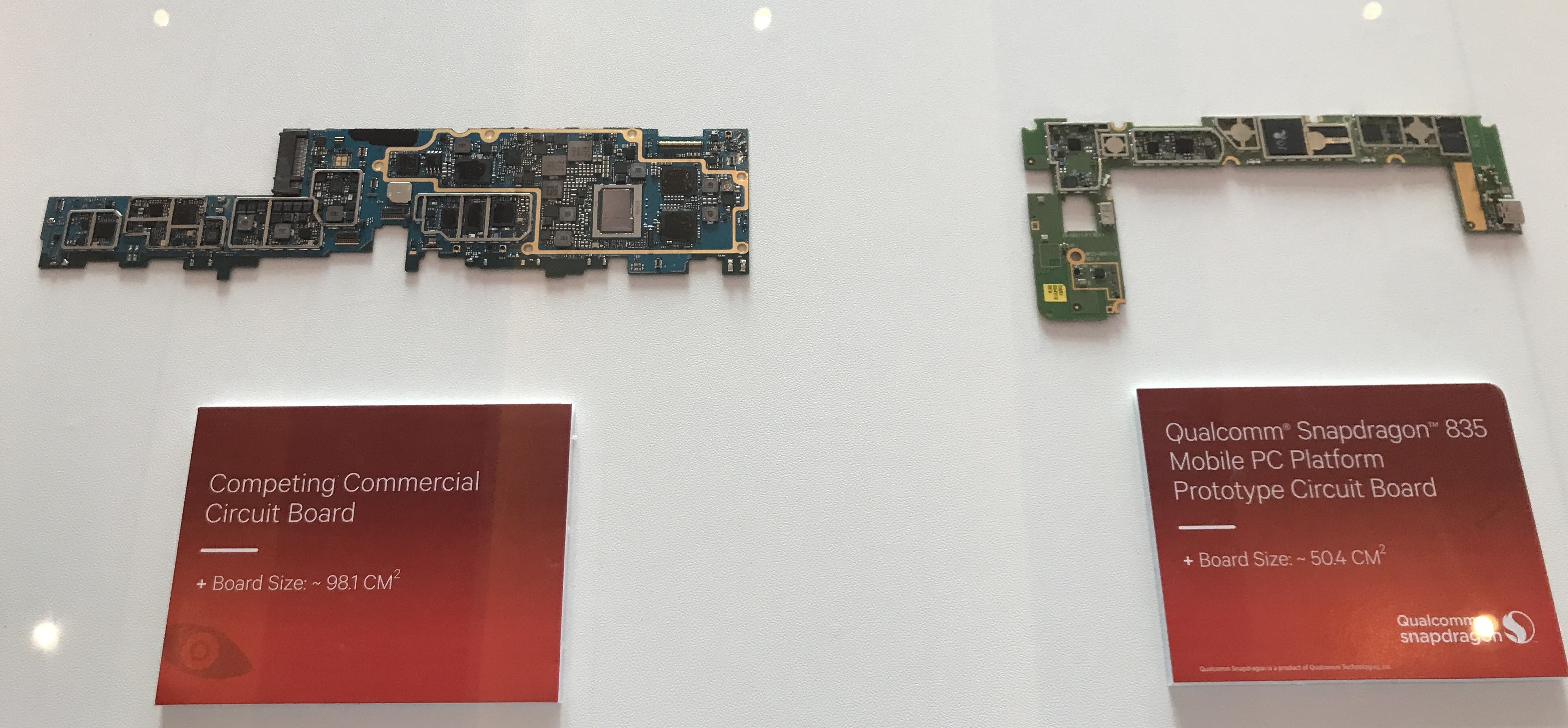
One of Qualcomm’s examples from 2018
For a Qualcomm processor designed for laptops, the silicon is a paired down to the essentials commonly associated with a smartphone. This means that modem connectivity is built into the processor, and the hardware associated with power delivery and USB are all on the scale of a smartphone. This means a motherboard designed around a Qualcomm processor will be around half the size, enabling different form factors, or more battery capacity in the same size laptop chassis.
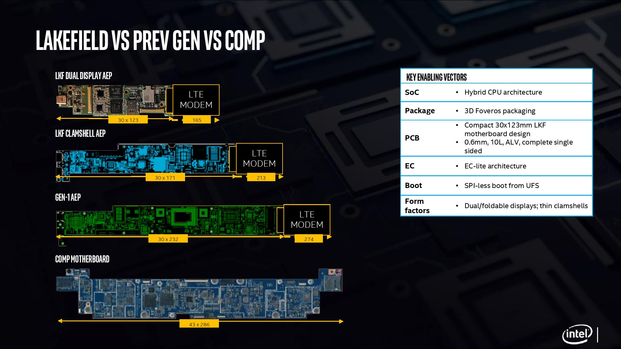
With Intel’s new Lakefield processor design, the chip is a lot smaller than previous Intel implementations. The company designed the processor from the ground up, with as much included on the CPU as to not need additional chips on the motherboard, and to fit the dimensions similar to one of Qualcomm’s processors. Above is a slide showing how Intel believes that with an LTE modem included, a Lakefield motherboard can move down to 7.7 square inches, similar to a Qualcomm design. This leaves more room for battery inside a device.
When Intel compares it against its own previous low power CPU implementations, the company quotes a 60% decrease in overall board area compared to its first generation 4.5 W processors.
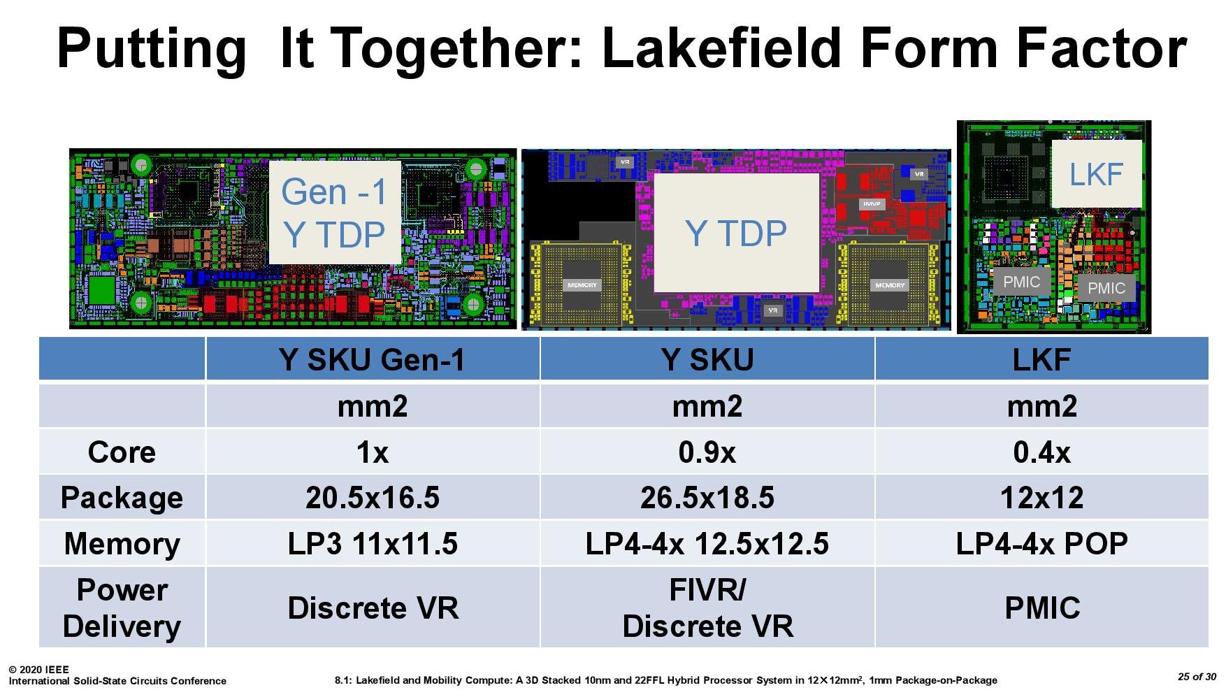
It is worth noting that for power delivery, Intel placed MIMCAPs inside the Lakefield silicon, much like a smartphone processor, and as a result it can get by on the power delivery implementation with a pair of PMICs (power management ICs). The reason why there is two is because of the two silicon dies inside – they are controlled differently for power for a number of technical reasons. If each layer within an active stacked implementation requires its own PMIC, that would presumably put an upper limit on future stacked designs – I fully expect Intel to be working on some sort of solution for this for it not to be an issue, however that wasn’t implemented in time for Lakefield.
For those that are interested, Lakefield’s PMICs are under the codenames Warren Cove and Castro Cover, and were developed in 2017-2018.


221 Comments
View All Comments
returnzer0 - Friday, July 3, 2020 - link
So no, they did not, in fact, read the same article.s.yu - Monday, July 6, 2020 - link
Mystery solved!vanilla_gorilla - Friday, July 3, 2020 - link
https://www.anandtech.com/show/15877/intel-hybrid-..."At the top is the single Sunny Cove core, also present in Ice Lake. Intel has stated that it has physically removed the AVX-512 part of the silicon, however we can still see it in the die shot. This is despite the fact that it can’t be used in this design due to one of the main limitations of a hybrid CPU. We’ll cover that more in a later topic."
It was NOT physically removed but it cannot be used so it doesn't really matter. In practice this will have no AVX-512.
dotjaz - Friday, July 3, 2020 - link
Also "However, all modern software assumes a homogeneous processor", that's why they have to support exactly the same ISA extensions. I didn't realise Windows is the only modern software in existence.Meteor2 - Friday, July 3, 2020 - link
Why so rude, dotjaz?dotjaz - Saturday, July 4, 2020 - link
So which part is rude? Is this rude asking you what's rude? Sorry your feelings got hurt. There, happy now?jospoortvliet - Sunday, July 5, 2020 - link
Linux also expects it. Modern enough?jeremyshaw - Thursday, July 2, 2020 - link
Good. This action ensures this segment of products will be easier to emulate on arm, helping to tear these products away from Intel's grasp.Kangal - Sunday, July 5, 2020 - link
To be honest, this is a great innovation.It's just the execution is quite lacking, and on top of that, it's a couple years too late.
Just imagine a SoC such as:
3x Big processor (Intel Core M), eg/ Core i7-8500Y
5x Small processor (Intel Atom), eg/ Atom x7-Z8750
Dynamic Scaling:
(Idle) 4x Small Cores run at 500MHz at Idle
(Very-low power) 4x Small Cores clock starting at 1.0GHz
(Low-power use) 5x Small Cores clock upto 2.5GHz
(Medium power) 3x Big Cores starting at 1.5GHz, 5x Small Cores upto 2.5GHz
(Regular power) 3x Big Cores at 2.0GHz, 5x Small Cores at 2.0GHz
(High-power use) 3x Big Cores at 3.0GHz, 5x Small Cores at 2.0GHz
(Very-high power) 3x Big Cores at 4.0GHz, 5x Small Cores at 2.5GHz
(Max-power use) 1x Big Cores at 5.0GHz, 2x Big Cores at 4.0GHz, 5x Small Cores at 2.5GHz
Kangal - Sunday, July 5, 2020 - link
Now imagine all of this, competing against AMD.Their 12nm node is fairly competitive against Intel's 14nm. And their Zen+ architecture is somewhat competitive against Intel's Skylake architecture. So comparing the above Hybrid Processor, to a 4c/8t (eg/ Ryzen-3780U). Well that's a no contest victory for Intel. And AMD would struggle to fit those technologies into a 8-core laptop processor, so there would be no threat from above.
Once AMD steps up to either Zen2 architecture, or 7nm node, or both!...
....that's when things get heated. Since in the 15W / Ultrabook market, the above setup by Intel would secure a slim victory against similar 4c/8t AMD processor. But when you step up to the 25W / Laptop market, then AMD will pull ahead with their 8c/16t processor. However at least in this scenario, Intel has a good showing of their competitiveness and capabilities. That works upto 2021, but after that, Intel will have to make noticeable performance improvements to both Big/Small Core architectures, AND, they will have to make substantial efficiency improvements on the lithography side (maybe execute on their 8nm nodes, versus TSMC's 5nm).
First question, why use examples of Cherry Trail and Amber Lake?
Well, they're both on Intel's (pretty good) 14nm node. Also this is the most efficient "Small Core" Atom architecture that Intel has. Later produced Intel Pentium/Celeron/Atom processors come from the same family, however, they're designed for higher energy consumption. Whereas the "Big Core" stated above is a Core M processor (now rebranded as a Core i7-Y), and it is the latest and best they have when it comes to performance whilst maintaining efficiency.
Why the 3/5 Split you may ask?
Well, the most useful is the first/main thread. Followed closely by the second thread as most code has evolved for Dual-Cores in the past 20 years. And somewhat important is the third core, as we've also had an evolution to Quad-Cores in the past 10 years. However, most code hasn't made the full transition from single to dual threads, the same way that dual threads haven't translated well to quad threads. So instead of 2+6 split, which will have some performance drops on Quad thread code, it's better to go for 3+5. So you may ask, then why not just go for an even 4+4 split? Well, most of those quad threads don't utilise the 4th core very well, so we can make do by relegating that to a Small Core instead. This saves us some efficiency, which is what we want to achieve with this concept in the first place. The least energy using split would be 0+8. The most performant split would be 8+0. So this 3+5 split is basically the best of both worlds, since you will get 90% of the single-threaded performance, 70% of the multi-threaded performance, and 50% of the energy expenditure characteristics. So it's not perfect, but it's the closest you can get there... until the code evolves further. And we've started transitioning codes running for 8-core processors only around 2015-2017, so there's a good chance we aren't going to see the evolution tipping point until around 2025.