The Intel Lakefield Deep Dive: Everything To Know About the First x86 Hybrid CPU
by Dr. Ian Cutress on July 2, 2020 9:00 AM ESTThermal Management on Stacked Silicon
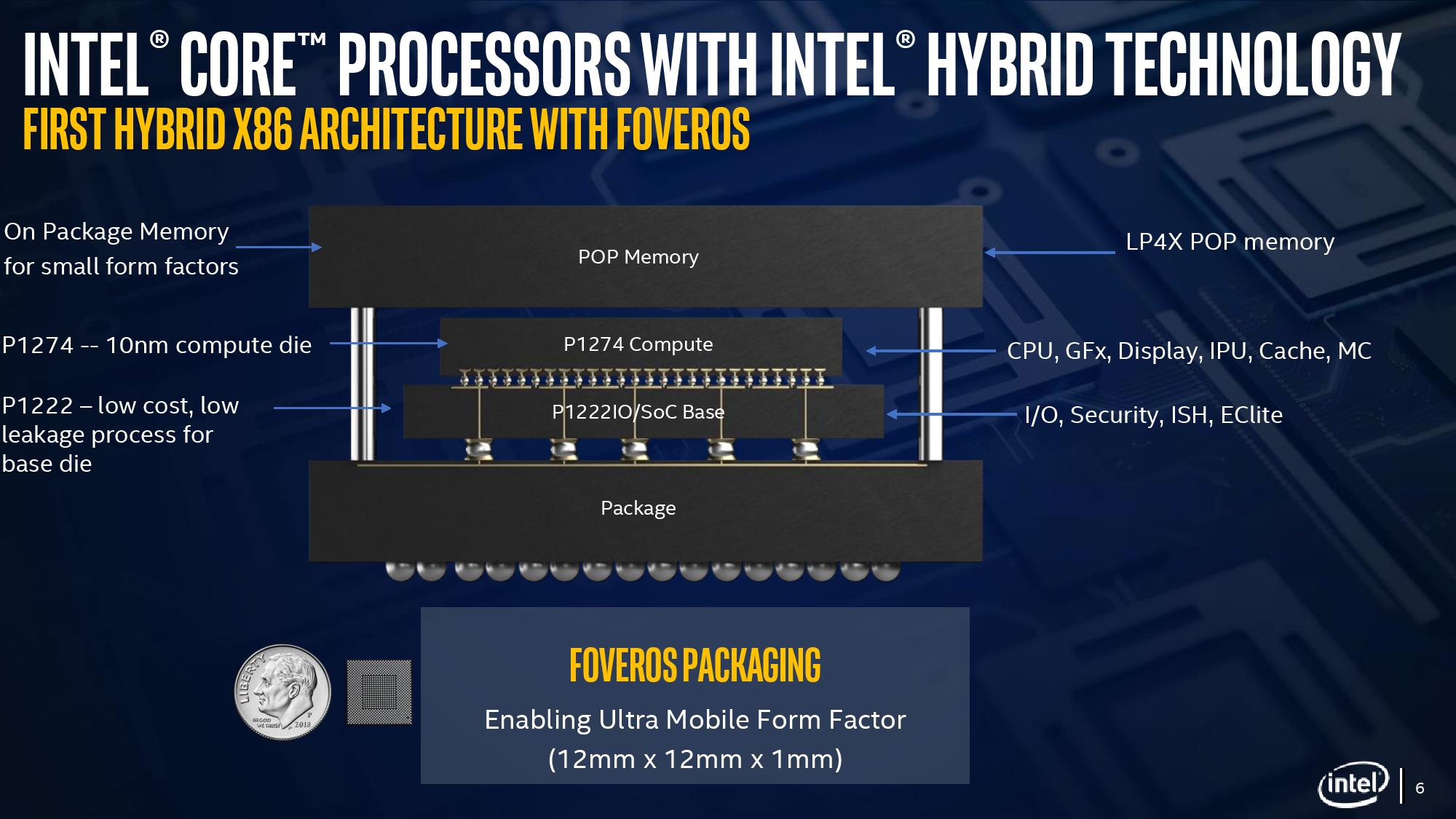
With a standard processor design, there is a single piece of silicon doing all the work and generating the heat – it’s bonded to the package (which doesn’t do any work) and then depending on the implementation, there’s some adhesive to either a cooler or a headspreader then a cooler. When moving to a stacked chiplet design, it gets a bit more complicated.
Having two bits of silicon that ‘do work’, even if one is the heavy compute die and the other is an active interposer taking care of USB and audio and things, does mean that there’s a thermal gradient between the silicon, and depending on the bonding, potential for thermal hotspots and build-up. Lakefield makes it even more complex, by having an additional DRAM package placed on top but not directly bonded.
We can take each of these issues independently. For the case of die-on-die interaction, there is a lot of research going into this area. Discussions and development about fluidic channels between two hot silicon dies have been going on for a decade or longer in academia, and Intel has mentioned it a number of times, especially when relating to a potential solution of its new die-to-die stacking technology.
They key here is hot dies, with thermal hotspots. As with a standard silicon design, ideally it is best to keep two high-powered areas separate, as it gives a number of benefits with power delivery, cooling, and signal integrity. With a stacked die, it is best to not have hotspots directly on top of each other, for similar reasons. Despite Intel using its leading edge 10+ process node for the compute die, the base die is using 22FFL, which is Intel’s low power implementation of its 14nm process. Not only that, but the base die is only dealing with IO, such as USB and PCIe 3.0, which is essentially fixed bandwidth and energy costs. What we have here is a high-powered die on top of a low powered die, and as such thermal issues between the two silicon die, especially in a low TDP device like Lakefield (7W TDP), are not an issue.
What is an issue is how the compute die gets rid of the heat. On the bottom it can do convection by being bonded to more silicon, but the top is ultimately blocked by that DRAM die. As you can see in the image above, there’s a big air gap between the two.
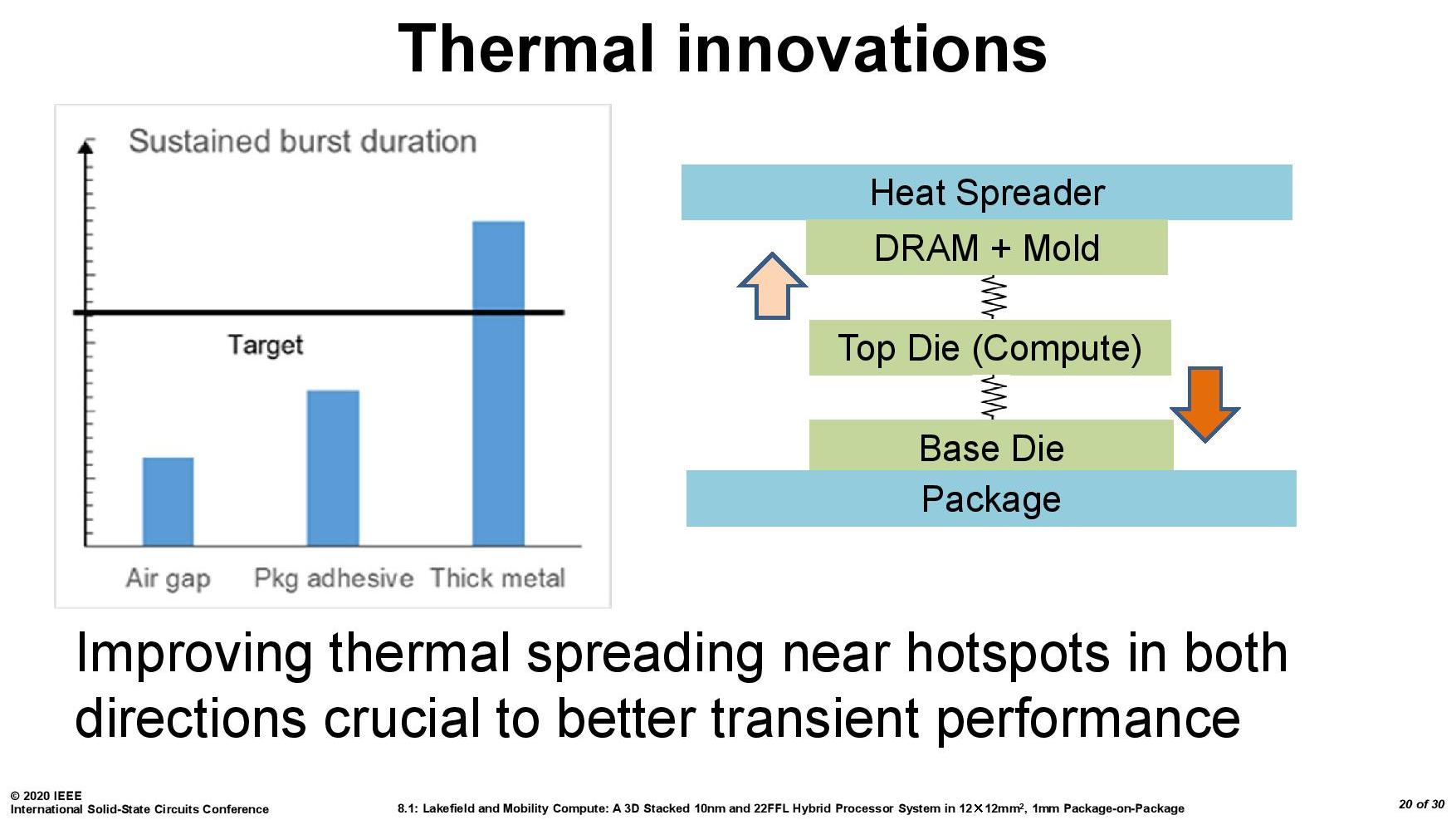
As part of the Lakefield design, Intel had to add in a number of design changes in order to make the thermals work. A lot of work can be done with the silicon design itself, such as matching up hotspots in the right area, using suitable thickness of metals in various layers, and rearranging the floorplan to reduce localized power density. Ultimately both increasing the thermal mass and the potential dissipation becomes high priorities.
Lakefield CPUs have a sustained power limit of 7 watts – this is defined in the specifications. Intel also has another limit, known as the turbo power limit. At Intel’s Architecture Day, the company stated that the turbo power limit was 27 watts, however in the recent product briefing, we were told is set at 9.5 W. Historically Intel will let its OEM partners (Samsung, Lenovo, Microsoft) choose its own values for these based on how well the design implements its cooling – passive vs active and heatsink mass and things like this. Intel also has another factor of turbo time, essentially a measure of how long the turbo power can be sustained for.
When we initially asked Intel for this value, they refused to tell us, stating that it is proprietary information. After I asked again after a group call on the product, I got the same answer, despite the fact that I informed the Lakefield team that Intel has historically given this information out. Later on, I found out through my European peers that in a separate briefing, they gave the value of 28 seconds, to which Intel emailed me this several hours afterwards. This value can also be set by OEMs.
Then I subsequently found one of Intel’s ISSCC slides.
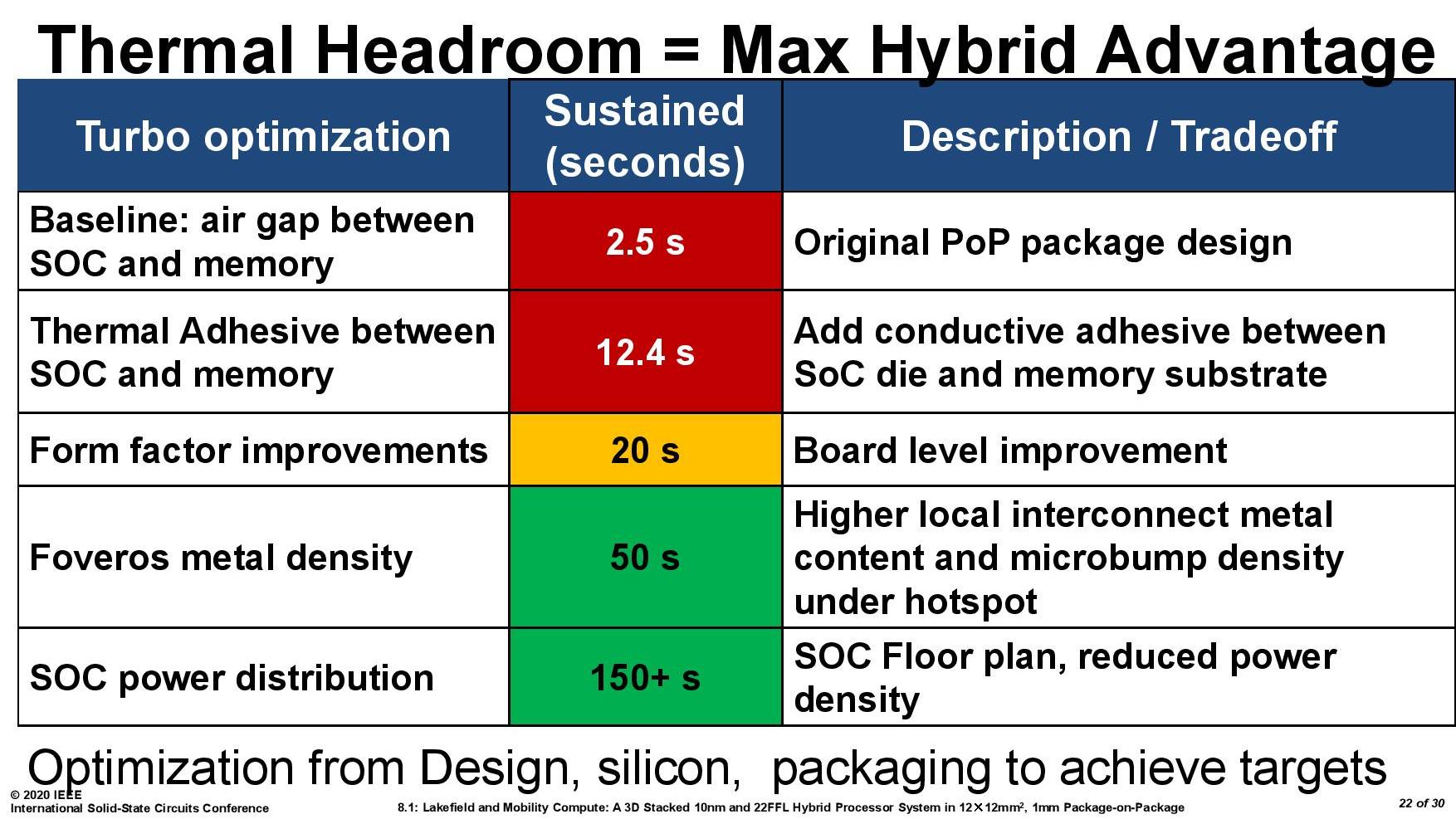
This slide shows that a basic implementation would only allow sustained power for 2.5 seconds. Adding in an adhesive between the top die and the DRAM moves up to 12.4 seconds, and then improving the system cooling goes up to 20 seconds. The rest of the improvements work below the compute die: a sizeable improvement comes from increasing the die-to-die metal density, and then an optimized power floor plan which in total gives sustained power support for 150+ seconds.


221 Comments
View All Comments
Spunjji - Monday, July 6, 2020 - link
That's the exact impression I got, too. They seems to be jumping around waving "look, we can do this too" when really it would have made far more practical sense *not to do it*.watzupken - Sunday, July 5, 2020 - link
Conceptually, this is a good way to lower power requirements to make Intel more competitive against ARM SOCs. However I agree that this is indeed for part smartphone, and part PC. Which unfortunately also means it may not be good for either one. From a smartphone perspective, while this may be a low power chip, but I am still not convinced that an x86 chips can be as efficient as a high end ARM chip. On the PC/ laptop space, I feel it will be more economical to just go for the pure Tremont based chips which should offer sufficient performance for light chores, and still offer good battery life. In my opinion, this is going to be a very niche chip and likely won't be cheap either.Farfolomew - Monday, July 6, 2020 - link
The engineers for this got screwed over by the marketing teams. There is no way this is supposed to compete with higher-end Core chips. It's supposed to be the New Atom replacement: It's supposed to fix everything that was wrong with previous 0+4 Atom CPUs: sluggish OS response and, to an extent, slow single-threaded perf. And also a boost in GPU capabilities.I hope Intel doesn't abandon this, even though, as Ian said, this first gen is going to get slammed
serendip - Tuesday, July 7, 2020 - link
I think Intel should have gone the other way by bringing Sunny Cove idle power down to ARM levels, instead of making this Frankenstein's monster of a chip. ARM licensees all use big cores to speed up UI threads and OS response but Intel seems to be using little Tremont Atom cores for everything. An upgrade to Atom wouldn't have saved Intel's position in mobile, not when ARM big cores have higher perf/watt.PandaBear - Monday, July 6, 2020 - link
Did I see $2499 for the Lenovo? Holy smoke, it is going to fail with this kind of processor. I think Intel is doomed with this being done on 10nm.hanselltc - Monday, July 6, 2020 - link
How does Comet lake fit into that power/performance graph?qwertymac93 - Monday, July 6, 2020 - link
Those performance numbers have me shaking my head. Currently, the chip is acting more like a "1 OR 4" core, not a "1 AND 4" core design. I can't help but wonder if two "big" cores would have been both faster and more power efficient... Clearly this product is suffering from first-gen-itus. 2021 can't come soon enough for Intel.MS - Tuesday, July 7, 2020 - link
Another science project by someone who has a stake in the Atom design. Some things are so bad, it's impossible to kill them. Avoton, Covington, they were all terrible products and all you need to do is look at the performance/power graph to see that there isn't even a net power saving. It's like putting a Pinto engine into a Mustang and expecting better gas mileage. What are they thinking? Or are they? The only thing they missed is piggy backing a Larrabee.name99 - Tuesday, July 7, 2020 - link
"here’s what Intel did, with each connection operating at 500 mega-transfers per second. The key point on this slide is the power: 0.2 picojoules of energy consumed per bit transferred."It's worth comparing this to the competition. TSMC has LIPINCON which is not exactly identical (I don't believe TSMC has publicly demo'd a stacked version) but at the abstract level of "chiplet to chiplet communication" it's the same thing.
TSMC gets 0.56pJ of power, but at a substantially faster 8GT/s. I don't know the extent to which this would scale down if reduced to Intel speeds, and whether its energy costs would go down (or even up, but that seems unlikely) if it were operating vertically rather than horizontally through an RDL.
Point is Foveros is a branding more than a technology per se. It's Intel's way of performing a particular type of packaging, but as far as we can tell, the same style of packaging is available to anyone who uses eg TSMC, if it met their particular goals.
(So far it hasn't because Apple, QC, Huawei, etc, can fit their entire SoC on a single die, they don't need to go through these contortions to either reduce the die size or deal with the limited capabilities of their fabs...
That sounds snarky, but Lakefield is deeply fishy. Sure, you want to save area, but the target is a tablet, and Apple's tablet SoC's have been 120 to 150mm^2. You'd figure a single die Lakefield all on 10nm would fit in ~150mm62 or less. So???)
And Samsung? I would guess so, but I don't know.
Spunjji - Friday, July 10, 2020 - link
Apple aren't trying to squeeze all of their profit margins out of the CPU alone, though. That's the difference.This is Intel trying to preserve margins by using fancy packaging technology to increase yield (and thus both output and margins) on their increasingly capacity-constrained nodes.