The Intel Lakefield Deep Dive: Everything To Know About the First x86 Hybrid CPU
by Dr. Ian Cutress on July 2, 2020 9:00 AM ESTThermal Management on Stacked Silicon
With a standard processor design, there is a single piece of silicon doing all the work and generating the heat – it’s bonded to the package (which doesn’t do any work) and then depending on the implementation, there’s some adhesive to either a cooler or a headspreader then a cooler. When moving to a stacked chiplet design, it gets a bit more complicated.
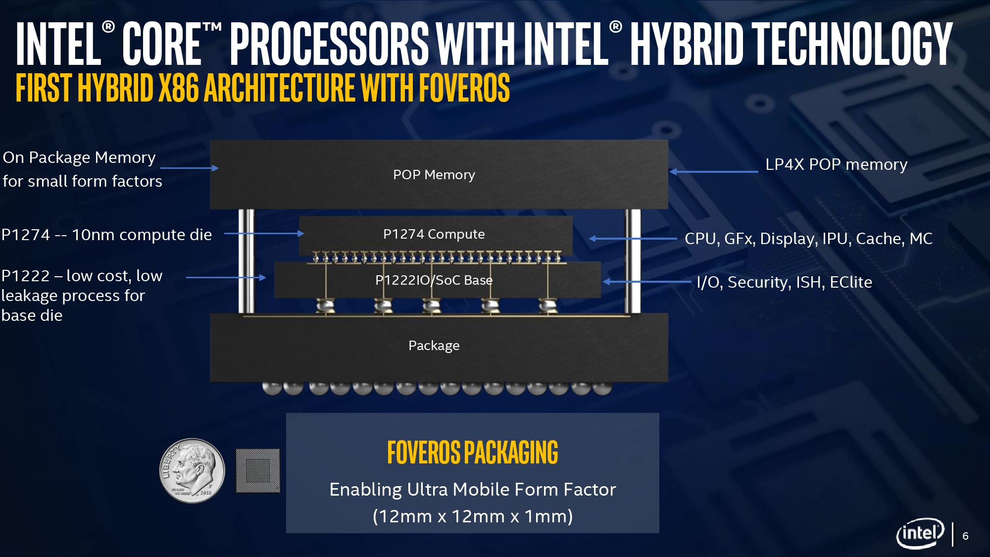
Having two bits of silicon that ‘do work’, even if one is the heavy compute die and the other is an active interposer taking care of USB and audio and things, does mean that there’s a thermal gradient between the silicon, and depending on the bonding, potential for thermal hotspots and build-up. Lakefield makes it even more complex, by having an additional DRAM package placed on top but not directly bonded.
We can take each of these issues independently. For the case of die-on-die interaction, there is a lot of research going into this area. Discussions and development about fluidic channels between two hot silicon dies have been going on for a decade or longer in academia, and Intel has mentioned it a number of times, especially when relating to a potential solution of its new die-to-die stacking technology.
They key here is hot dies, with thermal hotspots. As with a standard silicon design, ideally it is best to keep two high-powered areas separate, as it gives a number of benefits with power delivery, cooling, and signal integrity. With a stacked die, it is best to not have hotspots directly on top of each other, for similar reasons. Despite Intel using its leading edge 10+ process node for the compute die, the base die is using 22FFL, which is Intel’s low power implementation of its 14nm process. Not only that, but the base die is only dealing with IO, such as USB and PCIe 3.0, which is essentially fixed bandwidth and energy costs. What we have here is a high-powered die on top of a low powered die, and as such thermal issues between the two silicon die, especially in a low TDP device like Lakefield (7W TDP), are not an issue.
What is an issue is how the compute die gets rid of the heat. On the bottom it can do convection by being bonded to more silicon, but the top is ultimately blocked by that DRAM die. As you can see in the image above, there’s a big air gap between the two.
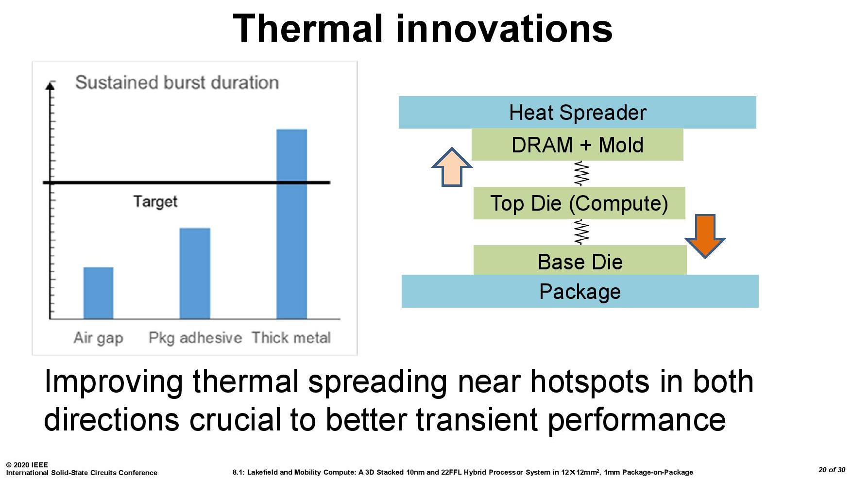
As part of the Lakefield design, Intel had to add in a number of design changes in order to make the thermals work. A lot of work can be done with the silicon design itself, such as matching up hotspots in the right area, using suitable thickness of metals in various layers, and rearranging the floorplan to reduce localized power density. Ultimately both increasing the thermal mass and the potential dissipation becomes high priorities.
Lakefield CPUs have a sustained power limit of 7 watts – this is defined in the specifications. Intel also has another limit, known as the turbo power limit. At Intel’s Architecture Day, the company stated that the turbo power limit was 27 watts, however in the recent product briefing, we were told is set at 9.5 W. Historically Intel will let its OEM partners (Samsung, Lenovo, Microsoft) choose its own values for these based on how well the design implements its cooling – passive vs active and heatsink mass and things like this. Intel also has another factor of turbo time, essentially a measure of how long the turbo power can be sustained for.
When we initially asked Intel for this value, they refused to tell us, stating that it is proprietary information. After I asked again after a group call on the product, I got the same answer, despite the fact that I informed the Lakefield team that Intel has historically given this information out. Later on, I found out through my European peers that in a separate briefing, they gave the value of 28 seconds, to which Intel emailed me this several hours afterwards. This value can also be set by OEMs.
Then I subsequently found one of Intel’s ISSCC slides.
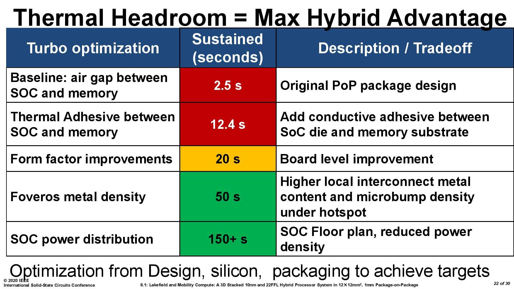
This slide shows that a basic implementation would only allow sustained power for 2.5 seconds. Adding in an adhesive between the top die and the DRAM moves up to 12.4 seconds, and then improving the system cooling goes up to 20 seconds. The rest of the improvements work below the compute die: a sizeable improvement comes from increasing the die-to-die metal density, and then an optimized power floor plan which in total gives sustained power support for 150+ seconds.


221 Comments
View All Comments
PaulHoule - Saturday, July 4, 2020 - link
@DrK,the engineering on this part is like what you'd get if you contracted out to Rockwell or Litton Industries for a brain for a Stinger missile. Compact, brilliantly packaged, with adequate performance, but no concern at all about thermal dissipation because the missile is going to hit or miss its target before the CPU fries.
Foveros is an expensive technology for a mass market device (cheap tablet) because the fabrication cost depends on the total area and there is an expensive step of stitching the chips together at the end. If you could avoid fabricating "glue" components and just snap together chips from a library this might be an amazing technology to build 500 of something at low development cost and time (e.g. weeks) If you have to make a new mask for the chip, however, it is a lot less fun.
So far as AVX the problem is as you say: "who cares about AVX?" Intel has shipped a backlog of features that people don't use because of overhead and complexity. As a software dev I get paid to work on certain aspect of my products, and maximizing performance with the latest instructions may or may not be on my agenda. If it is easy to do I will push for it but it means debugging compatibility problems it is a tough ask. "Optimal" performance for a range of users can mean shipping many versions of a function; the performance of loading, installing, updating, those libraries will be not in the least optimal.
Intel is like that Fatboy Slim album, 'We're #1, Why Try Harder?' The world has changed and Intel is not the #1 CPU firm any more. Intel has to get more Paranoid or it might not Survive.
Spunjji - Monday, July 6, 2020 - link
Why start with "I'm not one to criticise" and then do it? Clearly you are, and as a rhetorical flourish it's tedious in the extreme.1 - It's a first-gen product and it shows, but they're putting it in premium products.
2 - No deep-dive, for sure, but Intel's own figures are not very encouraging.
3 - Citation needed here. There's no sign of it being used outside of low-power premium devices.
4 - Who cares about AVX indeed! Tell that to the Intel fanboys pissing all over the AMD threads?
I'm entirely in favour of your final conclusion, but it's not really supported by the previous statements. 🤷♂️
Oxford Guy - Friday, July 3, 2020 - link
Bricklake or bust.Meteor2 - Friday, July 3, 2020 - link
Ultimately this is another attempt by Intel to stay relevant in a space where it's always struggled: mobile. With the progress being made by Apple, Microsoft, and Qualcomm using ARM, Intel is looking at losing an ever-growing chunk of what was the laptop market.But whatever Intel tries, bottom line is that ARM is more efficient than x86.
Beaver M. - Friday, July 3, 2020 - link
Thats not the issue. The issue is that theres not much software in that sector for x86.Valantar - Sunday, July 5, 2020 - link
A few errors in the article: 2 16-bit channels of LPDDR4X should be 2 32-bit channels of LPDDR4X, given that Renoir (with 4 32-bit LP4X channels at the same clock speed) delivers exactly 2x the bandwidth. Right?You should also proofread the pasted-in laptop descriptions; a lot of stuff in them clashes with the previous text.
Beyond that though: great article! Part of the reason why I love AT is for these technical yet understandable deep-dives. Looking forward to the next one.
Pixelpusher6 - Sunday, July 5, 2020 - link
Interesting choice to place the DRAM right over the core, seems like it would make more sense to move it next to the chip but on package. I guess my question is was it worth the complexity to implement this Foveros design to save a little space? It seems like they could have gotten the same benefit by using a traditional packaging i.e. with a little large package. Can you imagine paying $2500 like the price of that Lenovo and having Atom-esque performance?Pixelpusher6 - Sunday, July 5, 2020 - link
*largerFarfolomew - Monday, July 6, 2020 - link
Agreed on the DRAM placement. It seems really out of place. Another "dime size" piece of silicon right next to the Lakefield CPU doesn't seem like it would take up much more board space, and would alleviate a ton of the heat dissipation problems by allowing the compute-layer die to be directly connected to a heatsinkserendip - Monday, July 6, 2020 - link
It seems to be an interesting technical answer to a question nobody asked. Board space is a lot cheaper than what Lakefield would cost. It could also cost more for Intel to produce and they'd be stuck carrying multiple RAM SKUs.Heat dissipation could be a major issue. The slow chip could become even slower if it has to constantly throttle down because of thermal loads. Intel is sadly mistaken if this is supposed to be an ARM competitor.