The Intel Lakefield Deep Dive: Everything To Know About the First x86 Hybrid CPU
by Dr. Ian Cutress on July 2, 2020 9:00 AM ESTHybrid CPUs: Sunny Cove and Tremont
Now that we’ve gone over the concept of the heterogeneous core design, it’s time to dig into each of the cores separately and some of the tradeoffs that Intel has had to do in order to get this to work.
Big Sunny Cove
As mentioned previously, the big core in Lakefield is known as Sunny Cove, and stands as the same core we currently see in Intel’s Ice Lake mobile processors today. It is officially Intel’s second 10nm-class core (the first one being the DOA Cannon Lake / Palm Cove), but the first one in mass production.
We have covered the Sunny Cove core microarchitecture in great detail, and you can read about it here:
Examining Intel's Ice Lake Processors: Taking a Bite of the Sunny Cove Microarchitecture
The quick recap is as follows.
Very similar to a Skylake design, except that:
- Better prefetchers and branch predictors
- +50% L1 Data Cache
- +100% L1 Store Bandwidth
- +100% L2 Cache w/improved L2 TLB
- +50% Micro-op Cache
- +25% uops/cycle into reorder buffer
- +57% reorder buffer size
- +25% execution ports
- AVX-512 with VNNI
The side effect of increasing the L1 Data cache size was a decrease in latency, with the L1-D moving to a 5-cycle rather than a 4-cycle. Normally that would sound like a 25% automatic speed drop, however the increased L1 size, L1 bandwidth, and L2 cache all help for an overall improvement.
Intel claimed that Sunny Cove should perform ~18% better clock-for-clock compared to a Skylake core design. In our initial review of Ice Lake, we compared the i7-1065G7 processor (Ice Lake) to the Core i9-9900K processor (Coffee Lake, a Skylake derivative), and saw a 19% increase in performance per clock, essentially matching Intel’s advertised numbers.
(However it should be noted that overall we didn’t see that much of an improvement at the overall chip and product level, because the Ice Lake ran at a lower frequency, which removed any raw clock speed gain.)
Small Tremont Atom
Arguably the Tremont core is the more interesting of the two in the Lakefield design. Lakefield will be the first consumer product built with a Tremont core inside, and as a result we have not had a chance to test it yet. But we have gone over the microarchitecture extensively in a previous article.
Intel's new Atom Microarchitecture: The Tremont Core in Lakefield
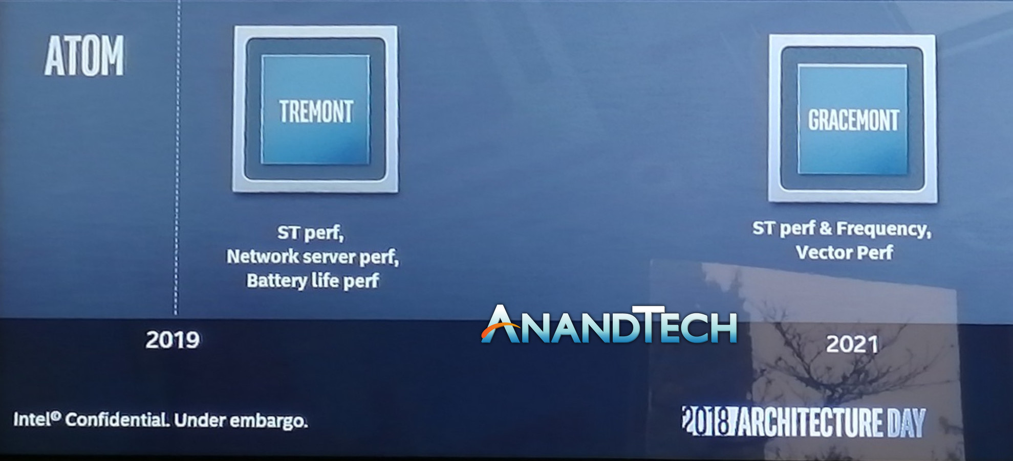
The reason why Tremont is more exciting is because updates to Intel’s Atom line of processor cores happen at a much slower pace. Traditionally Atom has been a core that focuses on the low cost part of the market, so there isn’t that much of a need to make it right at the bleeding edge as it commands lower margins for the company. It still plays a vital role, but for context, here is what year we’ve seen new Atom designs come into the market:
- 2008: Bonnell
- 2011: Saltwell
- 2013: Silvermont
- 2015: Airmont
- 2016: Goldmont
- 2017: Goldmont Plus
- 2020: Tremont
Tremont is the first new Atom microarchitecture design for three years, and technically only the third Atom design to be an out-of-order design. However, Tremont is a big jump in a lot of under-the-hood changes compared to Goldmont Plus.
- Can be in a 1-core, 2-core, or 4-core cluster
- +33% L1-Data Cache over Goldmont+, no performance penalty
- Configurable L2 cache per cluster, from 1.5 MB to 4.5 MB
- +50% L2 TLB (1024-entry, up from 512)
- New 2x3-wide decoder, rather than single 3-wide decoder
- +119% re-order buffer (208, up from 92)
- 8 execution ports, 7 reservation stations
- 3 ALUs, 2 AGUs
- Dual 128-bit AES units
- New Instructions*
What made the most noise is the new dual 3-wide decoder. On Intel’s primary Core line, we haven’t seen much change in the decoder in recent generations – it still uses a 5-wide decoder, split between 1 complex decoder and 4 simple decoders, backed with a micro-op cache. Tremont’s new dual 3-wide decoder can manage dual data streams in order to keep the buffers further down the core fed. Intel stated that for the design targets of Tremont, this was more area and power efficient than a 6-wide decoder, or having a large micro-op cache in the processor design (Atom cores have not have micro-op caches to date). Intel states that the decoder design helps shape the back-end of the core and the balance of resources.
Also worthy of note in Tremont is the L1-Data cache. Intel moved up from a 24 KiB design to a 32 KiB design, an increase of 33%. This is mostly due to using the latest manufacturing node. However, an increase in cache size is typically accompanied with an increase in latency – as we saw on Sunny Cove, we moved from a 4-cycle to a 5-cycle. However in Tremont’s case, the L1-Data cache stays at 3-cycle for an 8-way 32 KiB design. Even Skylake’s L1-D cache, at an 8-way 32 KiB design, is a 4-cycle, which means that Tremont’s L1-D is tuned to surpass even Skylake here.
The final point, Tremont’s new instructions, requires a section all on its own, specifically because none of the new instructions are supported in Lakefield.
What’s Missing in Lakefield
One of the biggest issues with a heterogeneous processor design is software. Even if we go beyond the issues that come with scheduling a workload on such a device, the problem is that most programs are designed to work on whatever microarchitecture they were written for. Generic programs are meant to work everywhere, while big publishers will write custom code for specific optimizations, such as if AVX-512 is detected, it will write AVX-512.
The hair-pulling out moment occurs when a processor has two different types of CPU core involved, and there is the potential for each of them to support different instructions or commands. Typically the scheduler makes no guarantee that software will run on any given core, so for example if you had some code written for AVX-512, it would happily run on an AVX-512 enabled core, but cause a critical fault on a core that doesn’t have AVX-512. The core won’t even know it’s an AVX-512 instruction until it comes time to decode it, and just throw an error when that happens. Not only this, but the scheduler has the right to move a thread when it needs to – if it moves a thread in the middle of an instruction stream, that can cause errors too. The processor could also move a thread to prevent thermal hotspots occurring, which will then cause a fault.
There could be a situation where the programmer can flag that their code has specific instructions. In a program with unique instructions, there’s very often a check that tries to detect support, in order to say to itself something like ‘AVX512 will work here!’. However, all modern software assumes a homogeneous processor – that all cores will support all of the same instructions.
It becomes a very chicken and egg problem, to a certain degree.
The only way out of this is that both processors in a hybrid CPU have to support the same instructions completely. This means that we end up with the worst of both worlds – only instructions supported by both can be enabled. This is the lowest common denominator of the two, and means that in Lakefield we lose support for AVX-512 on Sunny Cove, but also things like GFNI, ENCLV, and CLDEMOTE in Tremont (Tremont is actually rather progressive in its instruction support).
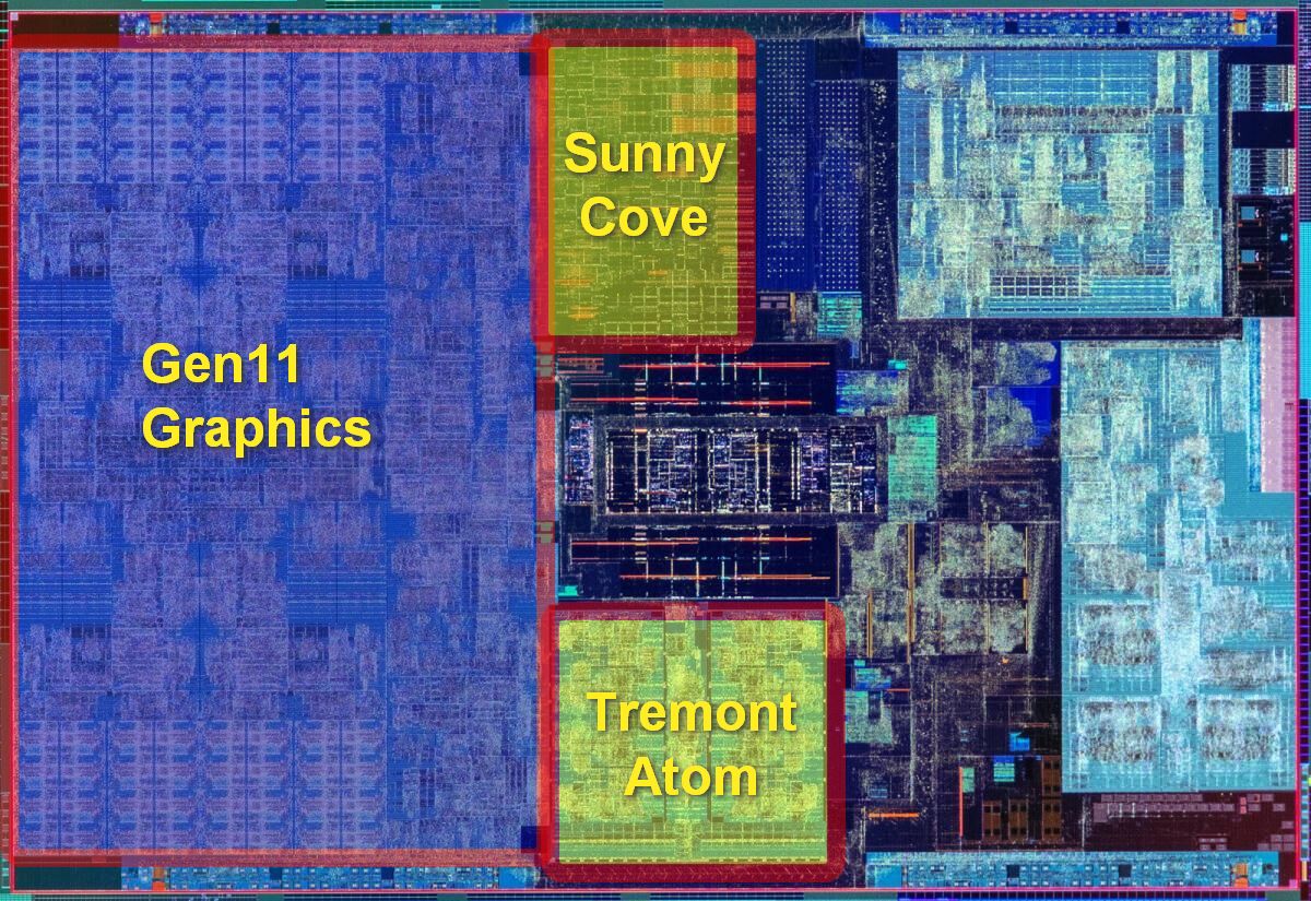
Knowing that Lakefield was going to have to take the lowest common denominator from the two core designs, Intel probably should physically removed the very bulky AVX-512 unit from the Sunny Cove core. Looking at the die shot, it's still there - there was some question going into the recent disclosures as to whether it would still be there, but Intel has stated on the record repeatedly that they removed it. The die shot of the compute silicon shows that not to be the case.
For x86 programmers doing instruction detection by code name or core family, this might have to change. In the smartphone world, where 4+4 processor designs are somewhat the norm, this lowest common denominator issue has essentially been universally adopted. There was some slight issue with a Samsung processor that had a non-unified cache setup, which ended up being rectified in firmware. But both sets of CPUs had to rely on lowest common denominator instructions.


221 Comments
View All Comments
Quantumz0d - Sunday, July 5, 2020 - link
PC gaming marketcap is supposed to be at $40Bn by 2022, total gaming market is $120Bn including everything, and Consoles are built on AMD x86 technology and now DX12U and you think that is a niche ?ARM is not going to do anything just because Apple did, there are so many trials by so many companies and the best company which is known for it's ROI with R&D, Qualcomm abandoned all of it's Server ARM marketshare dreams with the death of their full custom Centriq. x86 runs blazingly fast and optimized with Linux which is what the world is powered just because ARM is good in thin and light garbage doesn't make it a superstar.
ARM is not going to get into Desktop at all, no one is going to write their programs again to suppor that HW, and no company is going to invest in DIY market before Server/DC market. Supercomputer market is not the DIY or Enterprise, look at the Top Supercomputers, Chinese Tianhe and 2 positions are with Chinese only, AMD CRAY Zen based IF supercomputer is about to come as well.
Wilco1 - Sunday, July 5, 2020 - link
The #1 supercomputer is Arm, and Arm servers beat x86 servers on performance, cost and power, so not a single "fact" in your post is correct.lmcd - Sunday, July 5, 2020 - link
That first statement is hilariously disconnected from the second. Fugaku at 3x the cost per flop of its next competitor hardly backs up your assertion.ARM servers might beat x86 servers on performance, cost, and power but it's not looking that good vs x86_64. The latter arch is commodity hardware, software, and talent hiring.
Wilco1 - Monday, July 6, 2020 - link
Just looking at the peak FLOPS in comparisons is deceiving. Fugaku is a very different design as it does not use GPU accelerators like most supercomputers. That means it is far better than the rest in terms of ease of programming and efficiency. So even if the upfront cost is higher, they expect to get far more out of it than other super computers.I'd say Arm servers are doing really well in 2020, clearly companies want a change from the x86 duopoly. Much of the talent is at companies that do Arm designs. How else do you think Arm CPUs are getting 20-30% faster per year, and mobile phones already outperform the fastest x86 desktops?
Quantumz0d - Tuesday, July 7, 2020 - link
No company wants to develop an in house IP, that R&D and ROI is not easy, Amazon did it because to chop off some costs and set up a plan for the low end AWS instances with Graviton 2, Altera is still yet to show, Centriq abandoned by Qcomm with so much of marketing done around Cloudflare and top class engineering work, the team which made 820's full custom core.AND What the fuck you are babbling on fastest x86 desktops (Like Threadripper 3990X, or 3950X, 10900K) outperformed by mobile phones ? Ooof, you are gulping down the AT's SPEC scores aren't you ?
ARM servers LMAO, like how AMD upped their DC marketshare with EPYC7742, dude stop posting absolute rubbish. ARM marketshare in data centers is in 0.5% area where IBM also resides.
Quantumz0d - Monday, July 6, 2020 - link
Tiahu is fucking Chinese Sunway Processor based Supercomputer and it's top #3 so what did they do ? jack off to Zen with Hygon or did they make all Chinese use Chinese made processors ? Stop that bullshit of Supercomputer nonsense, IBM has been there since ages and they had SMT8 with Power9 uarch which came in 2017 (Summit which is #2, it was first since 2018) what did they do ? x86 is consumer based and DC market is relying only on that. ARM DC market-share is less than fucking 2%, AMD is at 4.5%, Intel is at 95% that is 2019 Q4.I don't know why people hate x86 as if it's like their life is being threatened by them, the fact that x86 machines are able to run vast diverse rich software selection and more freedom based computing, people want ARM based proprietary dogshit more, Apple series trash wich their APIs or the Bootloader locked (much worse like chastity) or Unlocked Android phones, even with GNU GPL v2 and Qcomm's top OSS CAF the godddamned phones do not get latest updates or anything but a Core2Quad from decade ago can run a fucking Linux or Win7 / Win10 without any bullshit issue.
Wait for the SPEC A series iPhone 12 benchmarks and then you be more proud of that garbage device which cannot compute anything outside what Apple deems it.
Wilco1 - Friday, July 3, 2020 - link
It would be good to run benchmarks on the 2 variants of Galaxy Book S. One comparison I found:https://browser.geekbench.com/v5/cpu/compare/25848...
So Lakefield wins by only 21% on single-threaded (that's a bad result given it is Cortex-A76 vs IceLake at similar clocks), and is totally outclassed on multithreaded...
lmcd - Sunday, July 5, 2020 - link
Current scheduler doesn't even guarantee that's the Sunny Cove core.Wilco1 - Monday, July 6, 2020 - link
Given Tremont can't get anywhere near Cortex-A76 performance, we can be sure single-threaded result is the Sunny Cove core.PaulHoule - Friday, July 3, 2020 - link
This is an example of the "Innovator's Dilemma" scenario where it is harder to move upmarket (in terms of performance) than downmarket.Put a phone processor into a box with a fan and people will be blown away by how fast it is -- they've never seen an ARM processor cooled by a fan before.
Put a desktop processor into a thin tablet with little thermal headroom and people will be blown away by how slow it is.
So first it is a situation that Intel can't win, but second it is a disaster that this low performance (downmarket) chip is expensive to produce and has to be sold upmarket. Sure you can stick any number of dies together and "scale up" a package in a way that looks as if you scaled up the chip by reducing the feature size, but when you reduce the feature size the cost per feature goes down in the long term -- when you stick a bunch of cheap chips together you get an expensive chip.