The Intel Lakefield Deep Dive: Everything To Know About the First x86 Hybrid CPU
by Dr. Ian Cutress on July 2, 2020 9:00 AM ESTThermal Management on Stacked Silicon
With a standard processor design, there is a single piece of silicon doing all the work and generating the heat – it’s bonded to the package (which doesn’t do any work) and then depending on the implementation, there’s some adhesive to either a cooler or a headspreader then a cooler. When moving to a stacked chiplet design, it gets a bit more complicated.
Having two bits of silicon that ‘do work’, even if one is the heavy compute die and the other is an active interposer taking care of USB and audio and things, does mean that there’s a thermal gradient between the silicon, and depending on the bonding, potential for thermal hotspots and build-up. Lakefield makes it even more complex, by having an additional DRAM package placed on top but not directly bonded.
We can take each of these issues independently. For the case of die-on-die interaction, there is a lot of research going into this area. Discussions and development about fluidic channels between two hot silicon dies have been going on for a decade or longer in academia, and Intel has mentioned it a number of times, especially when relating to a potential solution of its new die-to-die stacking technology.
They key here is hot dies, with thermal hotspots. As with a standard silicon design, ideally it is best to keep two high-powered areas separate, as it gives a number of benefits with power delivery, cooling, and signal integrity. With a stacked die, it is best to not have hotspots directly on top of each other, for similar reasons. Despite Intel using its leading edge 10+ process node for the compute die, the base die is using 22FFL, which is Intel’s low power implementation of its 14nm process. Not only that, but the base die is only dealing with IO, such as USB and PCIe 3.0, which is essentially fixed bandwidth and energy costs. What we have here is a high-powered die on top of a low powered die, and as such thermal issues between the two silicon die, especially in a low TDP device like Lakefield (7W TDP), are not an issue.
What is an issue is how the compute die gets rid of the heat. On the bottom it can do convection by being bonded to more silicon, but the top is ultimately blocked by that DRAM die. As you can see in the image above, there’s a big air gap between the two.
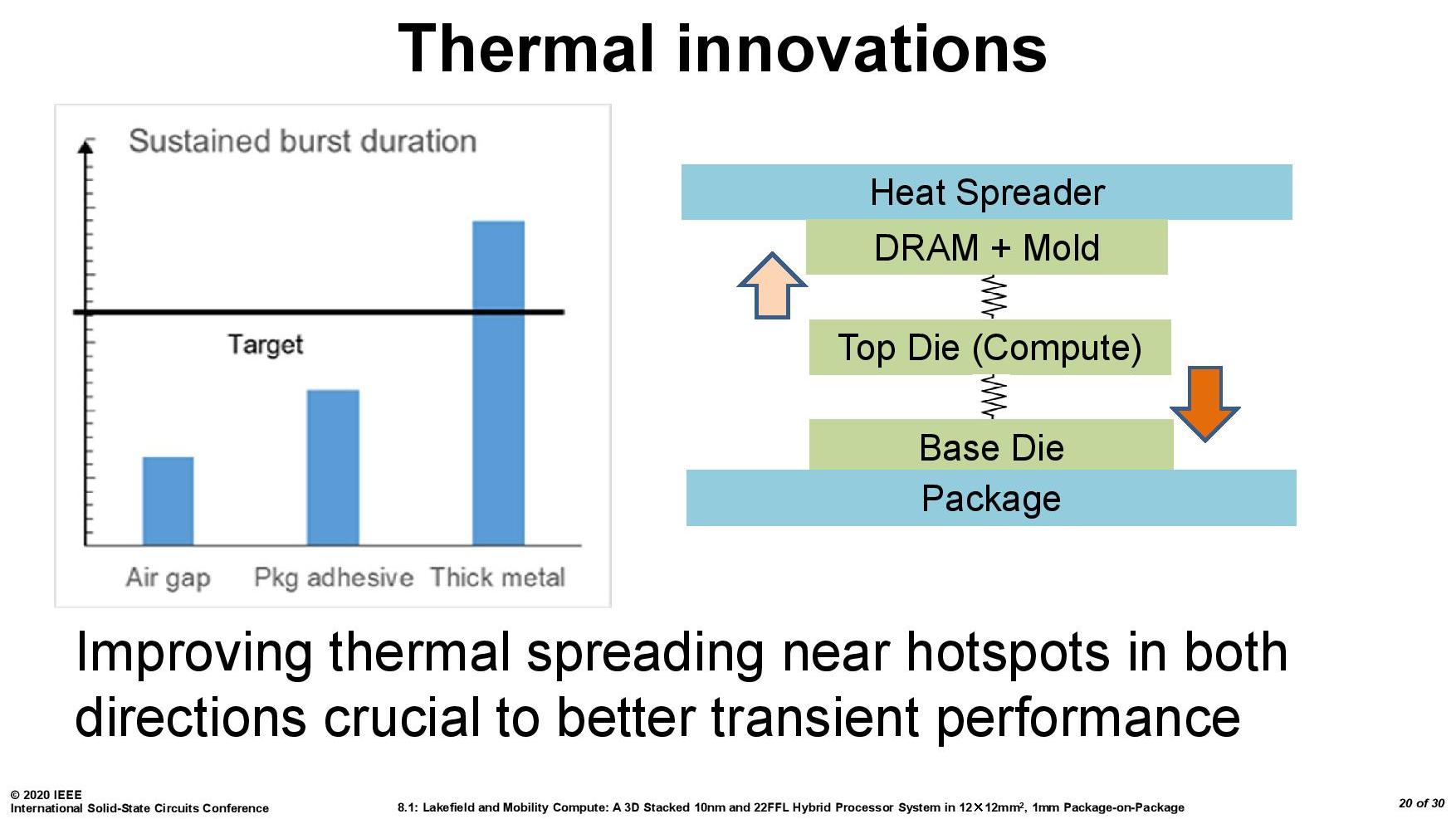
As part of the Lakefield design, Intel had to add in a number of design changes in order to make the thermals work. A lot of work can be done with the silicon design itself, such as matching up hotspots in the right area, using suitable thickness of metals in various layers, and rearranging the floorplan to reduce localized power density. Ultimately both increasing the thermal mass and the potential dissipation becomes high priorities.
Lakefield CPUs have a sustained power limit of 7 watts – this is defined in the specifications. Intel also has another limit, known as the turbo power limit. At Intel’s Architecture Day, the company stated that the turbo power limit was 27 watts, however in the recent product briefing, we were told is set at 9.5 W. Historically Intel will let its OEM partners (Samsung, Lenovo, Microsoft) choose its own values for these based on how well the design implements its cooling – passive vs active and heatsink mass and things like this. Intel also has another factor of turbo time, essentially a measure of how long the turbo power can be sustained for.
When we initially asked Intel for this value, they refused to tell us, stating that it is proprietary information. After I asked again after a group call on the product, I got the same answer, despite the fact that I informed the Lakefield team that Intel has historically given this information out. Later on, I found out through my European peers that in a separate briefing, they gave the value of 28 seconds, to which Intel emailed me this several hours afterwards. This value can also be set by OEMs.
Then I subsequently found one of Intel’s ISSCC slides.
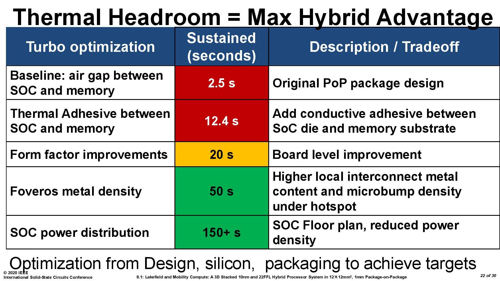
This slide shows that a basic implementation would only allow sustained power for 2.5 seconds. Adding in an adhesive between the top die and the DRAM moves up to 12.4 seconds, and then improving the system cooling goes up to 20 seconds. The rest of the improvements work below the compute die: a sizeable improvement comes from increasing the die-to-die metal density, and then an optimized power floor plan which in total gives sustained power support for 150+ seconds.


221 Comments
View All Comments
Quantumz0d - Sunday, July 5, 2020 - link
PC gaming marketcap is supposed to be at $40Bn by 2022, total gaming market is $120Bn including everything, and Consoles are built on AMD x86 technology and now DX12U and you think that is a niche ?ARM is not going to do anything just because Apple did, there are so many trials by so many companies and the best company which is known for it's ROI with R&D, Qualcomm abandoned all of it's Server ARM marketshare dreams with the death of their full custom Centriq. x86 runs blazingly fast and optimized with Linux which is what the world is powered just because ARM is good in thin and light garbage doesn't make it a superstar.
ARM is not going to get into Desktop at all, no one is going to write their programs again to suppor that HW, and no company is going to invest in DIY market before Server/DC market. Supercomputer market is not the DIY or Enterprise, look at the Top Supercomputers, Chinese Tianhe and 2 positions are with Chinese only, AMD CRAY Zen based IF supercomputer is about to come as well.
Wilco1 - Sunday, July 5, 2020 - link
The #1 supercomputer is Arm, and Arm servers beat x86 servers on performance, cost and power, so not a single "fact" in your post is correct.lmcd - Sunday, July 5, 2020 - link
That first statement is hilariously disconnected from the second. Fugaku at 3x the cost per flop of its next competitor hardly backs up your assertion.ARM servers might beat x86 servers on performance, cost, and power but it's not looking that good vs x86_64. The latter arch is commodity hardware, software, and talent hiring.
Wilco1 - Monday, July 6, 2020 - link
Just looking at the peak FLOPS in comparisons is deceiving. Fugaku is a very different design as it does not use GPU accelerators like most supercomputers. That means it is far better than the rest in terms of ease of programming and efficiency. So even if the upfront cost is higher, they expect to get far more out of it than other super computers.I'd say Arm servers are doing really well in 2020, clearly companies want a change from the x86 duopoly. Much of the talent is at companies that do Arm designs. How else do you think Arm CPUs are getting 20-30% faster per year, and mobile phones already outperform the fastest x86 desktops?
Quantumz0d - Tuesday, July 7, 2020 - link
No company wants to develop an in house IP, that R&D and ROI is not easy, Amazon did it because to chop off some costs and set up a plan for the low end AWS instances with Graviton 2, Altera is still yet to show, Centriq abandoned by Qcomm with so much of marketing done around Cloudflare and top class engineering work, the team which made 820's full custom core.AND What the fuck you are babbling on fastest x86 desktops (Like Threadripper 3990X, or 3950X, 10900K) outperformed by mobile phones ? Ooof, you are gulping down the AT's SPEC scores aren't you ?
ARM servers LMAO, like how AMD upped their DC marketshare with EPYC7742, dude stop posting absolute rubbish. ARM marketshare in data centers is in 0.5% area where IBM also resides.
Quantumz0d - Monday, July 6, 2020 - link
Tiahu is fucking Chinese Sunway Processor based Supercomputer and it's top #3 so what did they do ? jack off to Zen with Hygon or did they make all Chinese use Chinese made processors ? Stop that bullshit of Supercomputer nonsense, IBM has been there since ages and they had SMT8 with Power9 uarch which came in 2017 (Summit which is #2, it was first since 2018) what did they do ? x86 is consumer based and DC market is relying only on that. ARM DC market-share is less than fucking 2%, AMD is at 4.5%, Intel is at 95% that is 2019 Q4.I don't know why people hate x86 as if it's like their life is being threatened by them, the fact that x86 machines are able to run vast diverse rich software selection and more freedom based computing, people want ARM based proprietary dogshit more, Apple series trash wich their APIs or the Bootloader locked (much worse like chastity) or Unlocked Android phones, even with GNU GPL v2 and Qcomm's top OSS CAF the godddamned phones do not get latest updates or anything but a Core2Quad from decade ago can run a fucking Linux or Win7 / Win10 without any bullshit issue.
Wait for the SPEC A series iPhone 12 benchmarks and then you be more proud of that garbage device which cannot compute anything outside what Apple deems it.
Wilco1 - Friday, July 3, 2020 - link
It would be good to run benchmarks on the 2 variants of Galaxy Book S. One comparison I found:https://browser.geekbench.com/v5/cpu/compare/25848...
So Lakefield wins by only 21% on single-threaded (that's a bad result given it is Cortex-A76 vs IceLake at similar clocks), and is totally outclassed on multithreaded...
lmcd - Sunday, July 5, 2020 - link
Current scheduler doesn't even guarantee that's the Sunny Cove core.Wilco1 - Monday, July 6, 2020 - link
Given Tremont can't get anywhere near Cortex-A76 performance, we can be sure single-threaded result is the Sunny Cove core.PaulHoule - Friday, July 3, 2020 - link
This is an example of the "Innovator's Dilemma" scenario where it is harder to move upmarket (in terms of performance) than downmarket.Put a phone processor into a box with a fan and people will be blown away by how fast it is -- they've never seen an ARM processor cooled by a fan before.
Put a desktop processor into a thin tablet with little thermal headroom and people will be blown away by how slow it is.
So first it is a situation that Intel can't win, but second it is a disaster that this low performance (downmarket) chip is expensive to produce and has to be sold upmarket. Sure you can stick any number of dies together and "scale up" a package in a way that looks as if you scaled up the chip by reducing the feature size, but when you reduce the feature size the cost per feature goes down in the long term -- when you stick a bunch of cheap chips together you get an expensive chip.