The Intel Lakefield Deep Dive: Everything To Know About the First x86 Hybrid CPU
by Dr. Ian Cutress on July 2, 2020 9:00 AM ESTThermal Management on Stacked Silicon
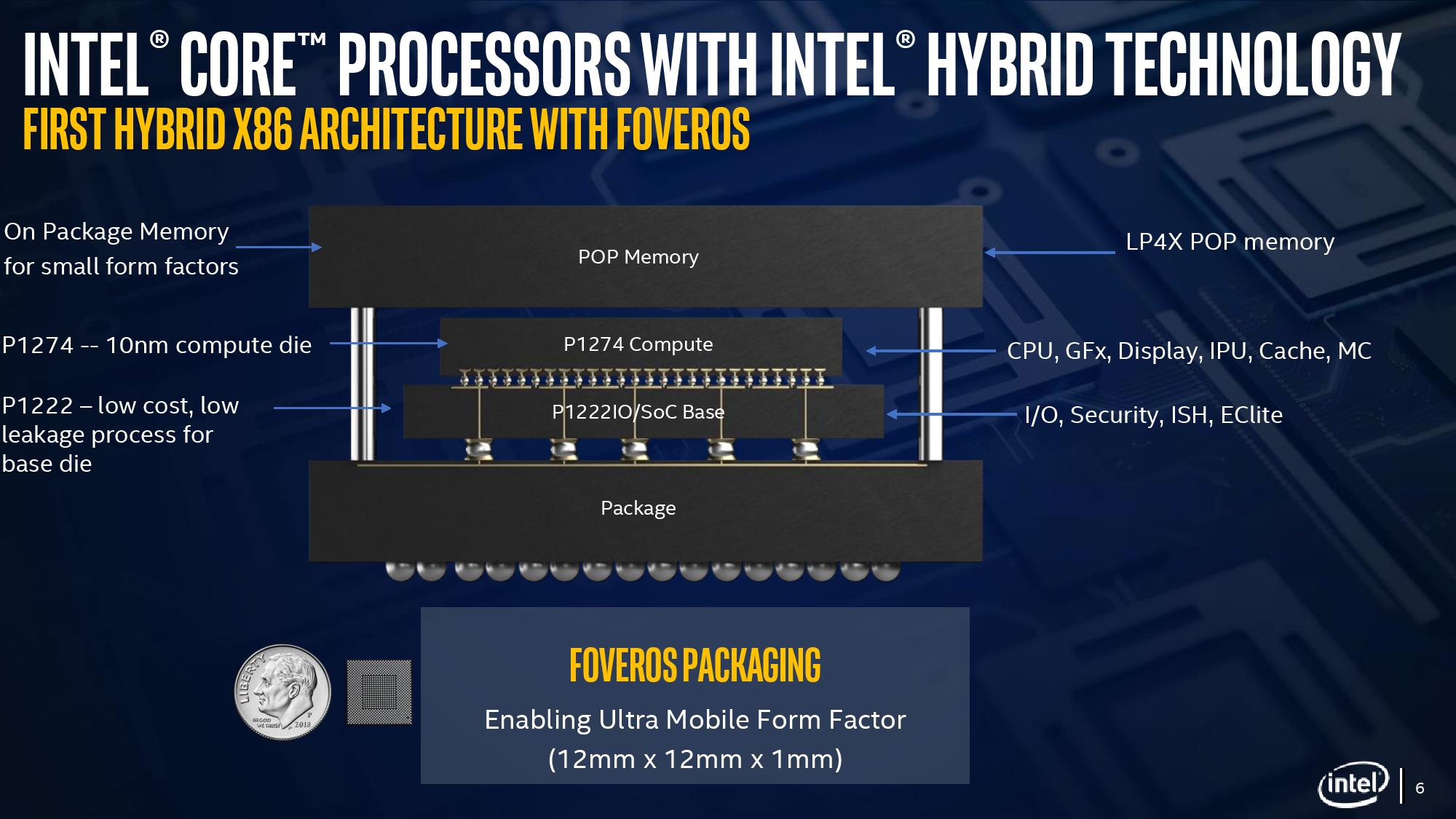
With a standard processor design, there is a single piece of silicon doing all the work and generating the heat – it’s bonded to the package (which doesn’t do any work) and then depending on the implementation, there’s some adhesive to either a cooler or a headspreader then a cooler. When moving to a stacked chiplet design, it gets a bit more complicated.
Having two bits of silicon that ‘do work’, even if one is the heavy compute die and the other is an active interposer taking care of USB and audio and things, does mean that there’s a thermal gradient between the silicon, and depending on the bonding, potential for thermal hotspots and build-up. Lakefield makes it even more complex, by having an additional DRAM package placed on top but not directly bonded.
We can take each of these issues independently. For the case of die-on-die interaction, there is a lot of research going into this area. Discussions and development about fluidic channels between two hot silicon dies have been going on for a decade or longer in academia, and Intel has mentioned it a number of times, especially when relating to a potential solution of its new die-to-die stacking technology.
They key here is hot dies, with thermal hotspots. As with a standard silicon design, ideally it is best to keep two high-powered areas separate, as it gives a number of benefits with power delivery, cooling, and signal integrity. With a stacked die, it is best to not have hotspots directly on top of each other, for similar reasons. Despite Intel using its leading edge 10+ process node for the compute die, the base die is using 22FFL, which is Intel’s low power implementation of its 14nm process. Not only that, but the base die is only dealing with IO, such as USB and PCIe 3.0, which is essentially fixed bandwidth and energy costs. What we have here is a high-powered die on top of a low powered die, and as such thermal issues between the two silicon die, especially in a low TDP device like Lakefield (7W TDP), are not an issue.
What is an issue is how the compute die gets rid of the heat. On the bottom it can do convection by being bonded to more silicon, but the top is ultimately blocked by that DRAM die. As you can see in the image above, there’s a big air gap between the two.
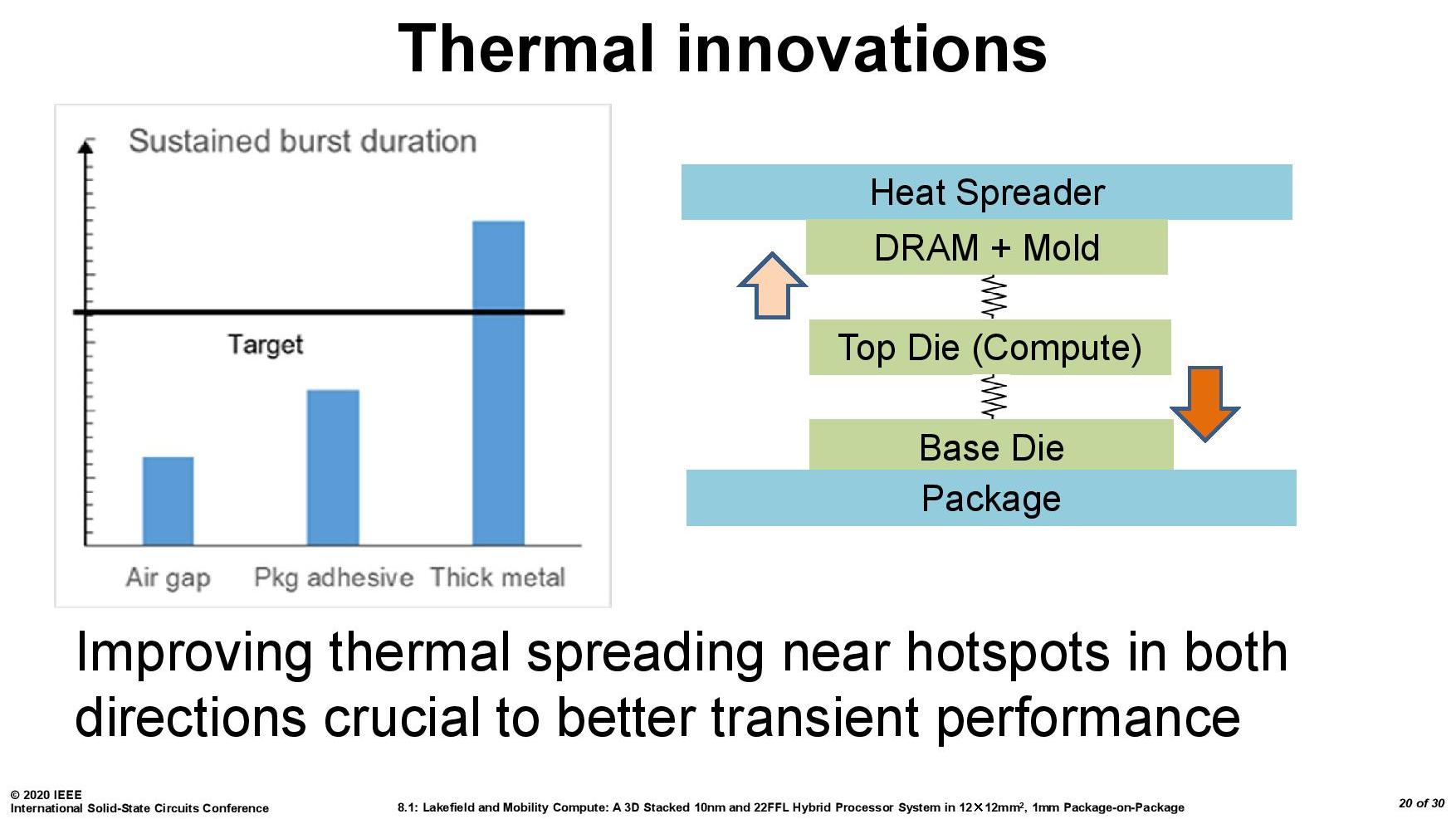
As part of the Lakefield design, Intel had to add in a number of design changes in order to make the thermals work. A lot of work can be done with the silicon design itself, such as matching up hotspots in the right area, using suitable thickness of metals in various layers, and rearranging the floorplan to reduce localized power density. Ultimately both increasing the thermal mass and the potential dissipation becomes high priorities.
Lakefield CPUs have a sustained power limit of 7 watts – this is defined in the specifications. Intel also has another limit, known as the turbo power limit. At Intel’s Architecture Day, the company stated that the turbo power limit was 27 watts, however in the recent product briefing, we were told is set at 9.5 W. Historically Intel will let its OEM partners (Samsung, Lenovo, Microsoft) choose its own values for these based on how well the design implements its cooling – passive vs active and heatsink mass and things like this. Intel also has another factor of turbo time, essentially a measure of how long the turbo power can be sustained for.
When we initially asked Intel for this value, they refused to tell us, stating that it is proprietary information. After I asked again after a group call on the product, I got the same answer, despite the fact that I informed the Lakefield team that Intel has historically given this information out. Later on, I found out through my European peers that in a separate briefing, they gave the value of 28 seconds, to which Intel emailed me this several hours afterwards. This value can also be set by OEMs.
Then I subsequently found one of Intel’s ISSCC slides.
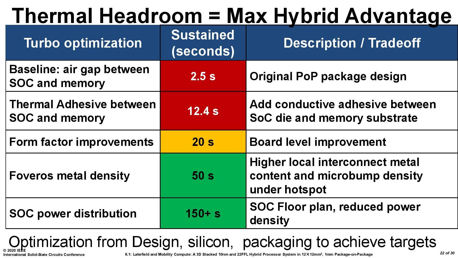
This slide shows that a basic implementation would only allow sustained power for 2.5 seconds. Adding in an adhesive between the top die and the DRAM moves up to 12.4 seconds, and then improving the system cooling goes up to 20 seconds. The rest of the improvements work below the compute die: a sizeable improvement comes from increasing the die-to-die metal density, and then an optimized power floor plan which in total gives sustained power support for 150+ seconds.


221 Comments
View All Comments
ichaya - Sunday, July 19, 2020 - link
SPEC is useful for some IPC comparisons, but it's questionable to use it for much else. PG bench in the phoronix link has a 50%+ speedup with SMT which is basically inline for perf/W/$ with Graviton 2 instance. The worst case is Casandra, but everything else is within ~5% for similar perf/$ if not comparable perf/W too since comparing TDP is workload dependent as well and not measured by most tests.XZ and Blender are ~45% faster with SMT in your openbenchmark link, but that's a 3900X (12-core/24-thread), so any comparisons to server chips (64-core Graviton 2) are unfair given power consumption and core differences. 4 times the L3 is also wrong, it's 50% more L2+L3 with half the cores and SMT if you're being fair between m6g.16xlarge or c6g.16xlarge and c5a.16xlarge.
Quantumz0d - Friday, July 3, 2020 - link
Intel has lost it's edge. And this whole portable nonsense is reaching peaks of stupidity. Those Lakefield processor equipped machines will be close to $1000 for their thin and ultra light 1 USB C / 1 3.5mm audio jack, what a fucking disaster.I had owned one ultrabook which is Acer Aspire S3 and I used to even play DotA2 on that, and after 1-2 years the whole machine heated like crazy, I repasted, no dice, cleaned fans, nothing. And then battery also stopped holding a charge. Now what ? That stupid POS is dead, not even worth, meanwhile a Haswell machine with rPGA socket, and an MXM slot from 2013 and guess what ? the GPU got an upgrade to Pascal 1070 MXM from Kepler 860M.
All these BGA trash machines will no longer hold charge nor have their serviceability, older ultrabooks atleast had a 2.5" drive, newer ones have NVMe SSDs, these 2 in 1 trash like most of the Surface lineup is almost impossible to even repair or service. And because of this thin and light market Windows 10 has been ruined as well to cater to this bs phenomenon and desktop class OS is hit with that ugly Mobile UX which lacks powerful software options, navigation and all. Plus you don't even get to repair it yourself due to non available servicing parts.
With Apple HW same thing, full BGA not even NVMe SSDs, and now they also started to make their Mac OS look and feel like iOS trash. This whole mobile and ultra portable garbage is ruining everything, from gaming to the HW.
PandaBear - Monday, July 6, 2020 - link
They don't want to cannibalize their highly profitable x86 business, so they have to give you crap for what you want if you want to pay less. The problem right now is other companies don't have to deal with this political monopoly BS and they are eating Intel for lunch.Most monopolies die this way: when their monopoly business is obsoleted and they hang on to it to milk the cow till it dies.
yeeeeman - Friday, July 3, 2020 - link
Tigerlake should also be in the pipeline soon, right?Deicidium369 - Saturday, July 4, 2020 - link
Benchmarks showing it destroying AMD Renoir at single core, and within 17% on MT - despite half the cores...https://wccftech.com/intel-10nm-core-i7-1165g7-cpu...
watzupken - Sunday, July 5, 2020 - link
"Benchmarks showing it destroying AMD Renoir at single core, and within 17% on MT - despite half the cores...https://wccftech.com/intel-10nm-core-i7-1165g7-cpu...
Till we see the actual performance, you need to take these leaks with a lot of salt. The test bed are not revealed in leaks and it is not possible to ascertain if it is a realistic number. This we don't have to speculate for long since it should be out pretty soon.
pugster - Friday, July 3, 2020 - link
Lakefield's 2.5w standby sounds kind of high. ARM cpu is probably much lower than that.Ian Cutress - Monday, July 20, 2020 - link
2.5 mWProDigit - Friday, July 3, 2020 - link
Qualcomm has proven that a single fast core isn't enough. Intel needs to at least do 2 fast cores. Then add at least 6 atom cores.But if Intel wants to compete with AMD, it'll need to create a quad core big setup, with at least 10 to 12 atom cores.
Any less will be too little. These are too little as is, competing against the 3000 series of AMD.
It would be awesome, if Intel could make a 25W quad core cpu, paired with an additional 40 watts on atom cores. That's about 20 additional cores, or a 24 core cpu.
abufrejoval - Friday, July 3, 2020 - link
A great article overall, very informative, deeply technical while still readable to a layman, very little judgement or marketing, allowing readers to form their own opinion: Anandtech at its very best!Not mentioned in the article and not covered by the comments so far is that the main driver behind Intel’s low power SoCs has been Apple: This is what Intel thought Apple would want and be happy with!
And if you contrast it to what Apple will now do on their own, that makes me want to sell all my Intel shares: Good thing I never had any.
This is another Intel 80432 or i860, tons of great ideas engineered into parts, but great parts don’t automatically make a convincing whole.
And I simply don’t see them iterate that into many more designs over the next years at competitive prices: With that hot-spot governed layout between the two all the flexibility and cost savings a chiplet design is supposed to deliver goes away and you now have two chips in a very tight symbiosis with no scale-up design benefits.
It’s a Foveros tech demo, but a super expensive one with very little chance of currying favors even at ‘negative revenues’ in the current market.
X86 is not competitive in terms of Watts or transistors required for a given amount of compute. It didn’t matter that much in PCs, the competing servers were much worse for a long time, but in the mobile space, phones to ultrabooks, it seems impossible to match ARM, even if you could rewind the clock by ten years and started to take BIG-little seriously. Lakefield is essentially a case study for Core being too big and thus power hungry and Atom failing on performance.
ISA legacy is still holding x86 from dying completely, but that matters less and less at both the top of the performance range with servers and at the bottom in mobile, where the Linux kernel rules supreme and many userlands and ISAs compile just fine.
Gaming is a hold-out, but perhaps the last generation consoles on x86, gamer PCs alone too much of a niche to determine the future.
The desktop will switch to who offers the bigger, longer lasting bang for the buck and there is a very good chance that will be ARM next.
Microsoft may be allowed to blunder along with lackluster ARM64 support for a couple more days, but Apple’s switch puts them under long deserved pressure. A nice Linux/Android/Chromium hybrid ultrabook running whatever Office could get things moving quicker… at least I hope that, because I’d never want to be forced into the bitten Apple…. by these corporate decision makers I see already twitching.
No chance I’d ever let a new Apple into my home: The ][ was the last good one they made.