The Intel Lakefield Deep Dive: Everything To Know About the First x86 Hybrid CPU
by Dr. Ian Cutress on July 2, 2020 9:00 AM ESTThermal Management on Stacked Silicon
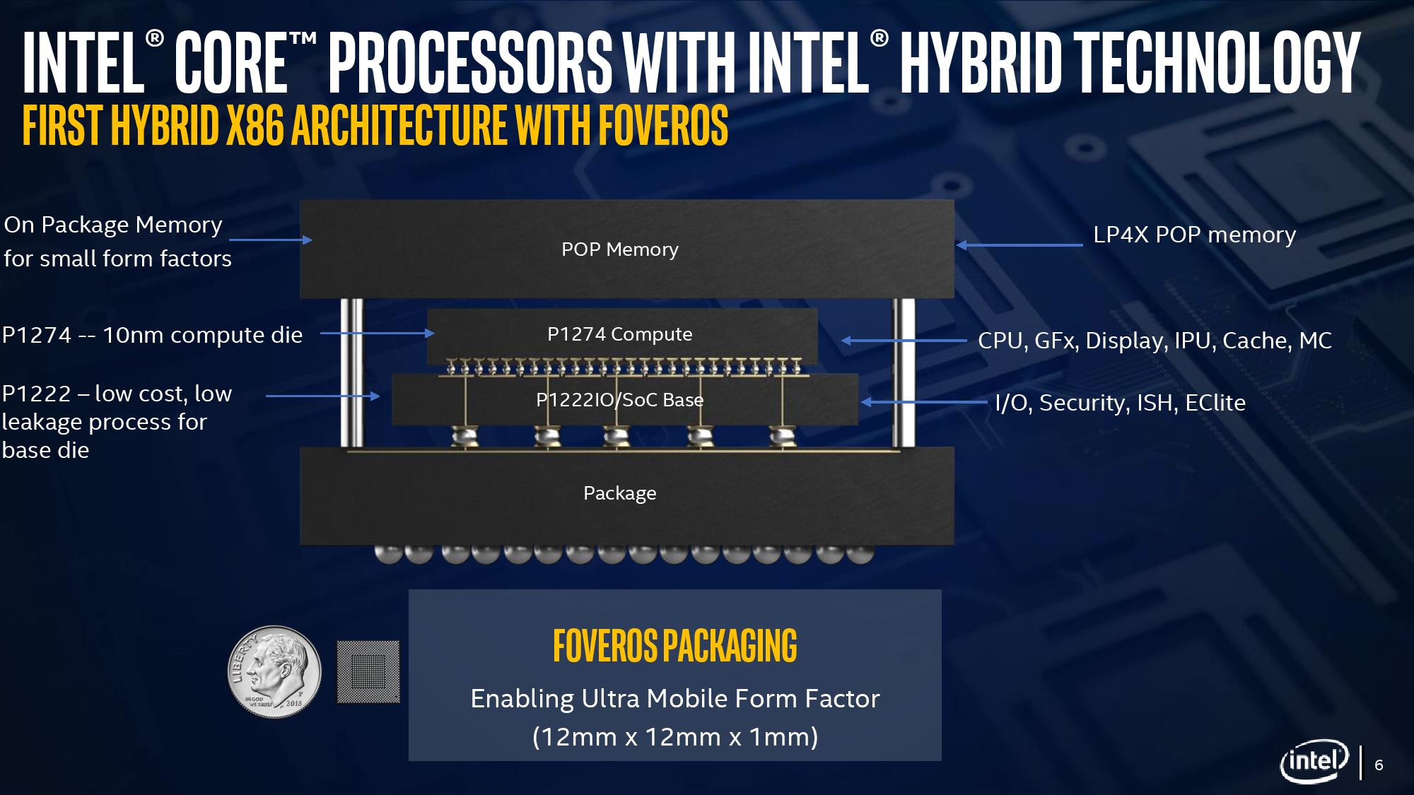
With a standard processor design, there is a single piece of silicon doing all the work and generating the heat – it’s bonded to the package (which doesn’t do any work) and then depending on the implementation, there’s some adhesive to either a cooler or a headspreader then a cooler. When moving to a stacked chiplet design, it gets a bit more complicated.
Having two bits of silicon that ‘do work’, even if one is the heavy compute die and the other is an active interposer taking care of USB and audio and things, does mean that there’s a thermal gradient between the silicon, and depending on the bonding, potential for thermal hotspots and build-up. Lakefield makes it even more complex, by having an additional DRAM package placed on top but not directly bonded.
We can take each of these issues independently. For the case of die-on-die interaction, there is a lot of research going into this area. Discussions and development about fluidic channels between two hot silicon dies have been going on for a decade or longer in academia, and Intel has mentioned it a number of times, especially when relating to a potential solution of its new die-to-die stacking technology.
They key here is hot dies, with thermal hotspots. As with a standard silicon design, ideally it is best to keep two high-powered areas separate, as it gives a number of benefits with power delivery, cooling, and signal integrity. With a stacked die, it is best to not have hotspots directly on top of each other, for similar reasons. Despite Intel using its leading edge 10+ process node for the compute die, the base die is using 22FFL, which is Intel’s low power implementation of its 14nm process. Not only that, but the base die is only dealing with IO, such as USB and PCIe 3.0, which is essentially fixed bandwidth and energy costs. What we have here is a high-powered die on top of a low powered die, and as such thermal issues between the two silicon die, especially in a low TDP device like Lakefield (7W TDP), are not an issue.
What is an issue is how the compute die gets rid of the heat. On the bottom it can do convection by being bonded to more silicon, but the top is ultimately blocked by that DRAM die. As you can see in the image above, there’s a big air gap between the two.
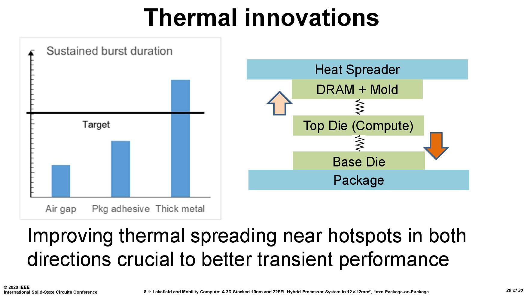
As part of the Lakefield design, Intel had to add in a number of design changes in order to make the thermals work. A lot of work can be done with the silicon design itself, such as matching up hotspots in the right area, using suitable thickness of metals in various layers, and rearranging the floorplan to reduce localized power density. Ultimately both increasing the thermal mass and the potential dissipation becomes high priorities.
Lakefield CPUs have a sustained power limit of 7 watts – this is defined in the specifications. Intel also has another limit, known as the turbo power limit. At Intel’s Architecture Day, the company stated that the turbo power limit was 27 watts, however in the recent product briefing, we were told is set at 9.5 W. Historically Intel will let its OEM partners (Samsung, Lenovo, Microsoft) choose its own values for these based on how well the design implements its cooling – passive vs active and heatsink mass and things like this. Intel also has another factor of turbo time, essentially a measure of how long the turbo power can be sustained for.
When we initially asked Intel for this value, they refused to tell us, stating that it is proprietary information. After I asked again after a group call on the product, I got the same answer, despite the fact that I informed the Lakefield team that Intel has historically given this information out. Later on, I found out through my European peers that in a separate briefing, they gave the value of 28 seconds, to which Intel emailed me this several hours afterwards. This value can also be set by OEMs.
Then I subsequently found one of Intel’s ISSCC slides.
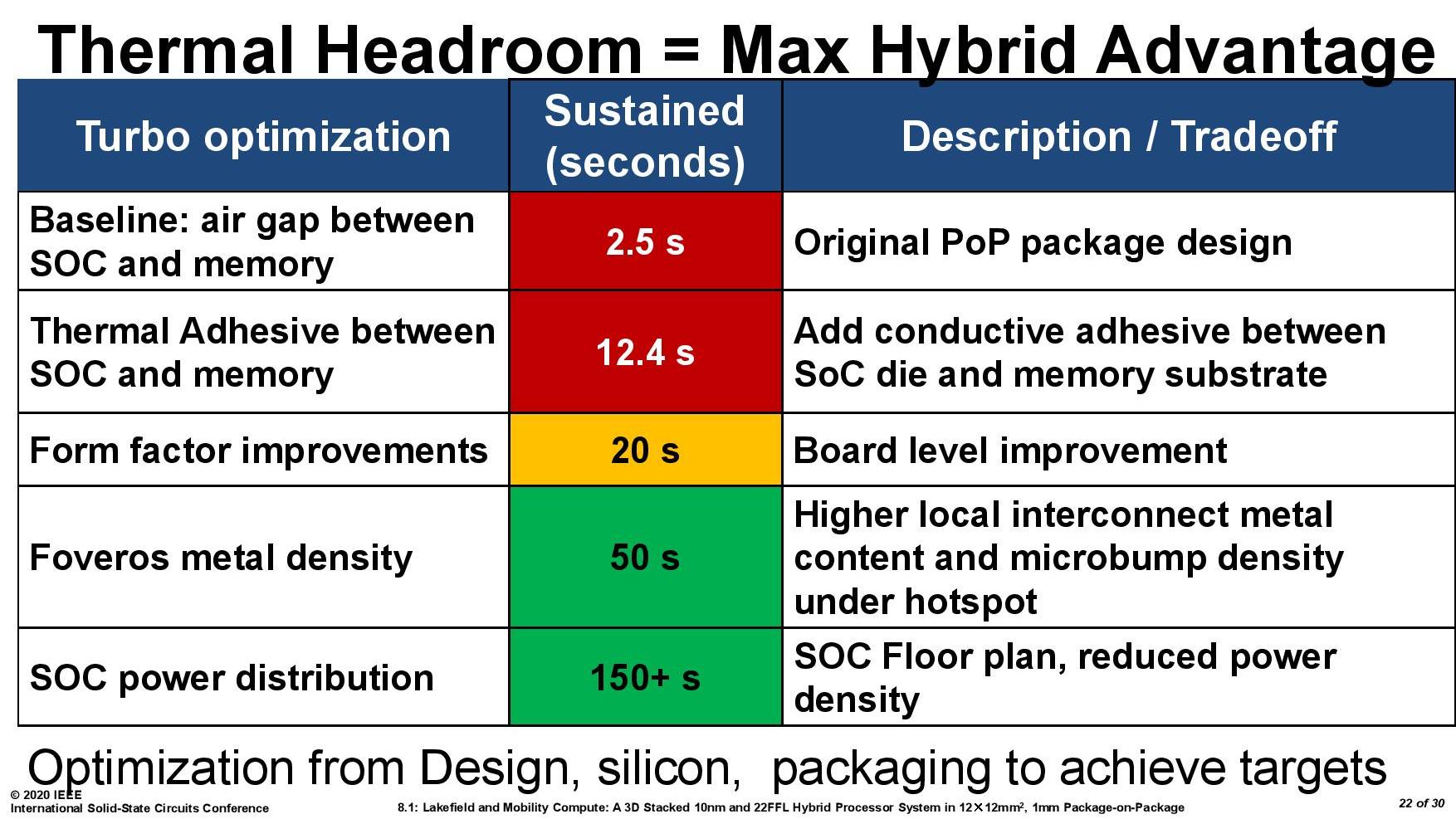
This slide shows that a basic implementation would only allow sustained power for 2.5 seconds. Adding in an adhesive between the top die and the DRAM moves up to 12.4 seconds, and then improving the system cooling goes up to 20 seconds. The rest of the improvements work below the compute die: a sizeable improvement comes from increasing the die-to-die metal density, and then an optimized power floor plan which in total gives sustained power support for 150+ seconds.


221 Comments
View All Comments
Alistair - Thursday, July 2, 2020 - link
The only point of this is if it is dirt cheap. You don't pay a premium for 1 core and 4 atom cores. DOA. I'll take a 7nm 4 core Zen 2 laptop instead thanks.Make this a $50 CPU? Then I'm interested.
lmcd - Thursday, July 2, 2020 - link
I don't think it'll be $50 but if it is, I hope to see it on single-board computers. That'd be slick.serendip - Thursday, July 2, 2020 - link
It's meant for $1000 computers, not cheap sub-$500 devices. I wouldn't pay that much money for 4 Atom cores and a big core that sits around like an unwanted appendage.lmcd - Friday, July 3, 2020 - link
It's meant for $1000 tablets and ultralights, not traditional computer form factors.Glad you won't buy any smartphone then!
yeeeeman - Friday, July 3, 2020 - link
Qualcomm is fighting in the same space with 8cx for the same huge prices and that one doesn't even run x64 apps. This market wants very light laptops with very good battery life and LKF does just that, wherever you like it or not.Spunjji - Monday, July 6, 2020 - link
We'll see what the market actually wants when this launches. I have a strong suspicion that the market doesn't want the absolutely miserable performance/$ on offer here, even for the quoted battery life benefits, but I've been wrong before.justing6 - Thursday, July 2, 2020 - link
Amazing article! I learned so much about Lakefield and 3D stacking in general. The technology and engineering is really incredible, but as a consumer product it looks extremely lacking.I'm a proud owner and heavy user of a Surface Pro X, and the 8cx/SQ1 is generally "good enough" when running ARM workloads. Going to a 15W Intel chip that can turbo to 25-40W feels noticeably snappier, but when considering the SQ1 is 7W-15W it's really impressive. The 4+4 also allows for very good multitasking performance, it takes 10GB+ of heavy web browser tabs running on an external 3440x1440p display before it really feels like it starts to slow down.
However, that's when I live inside Chromium Edge running native ARM64 code. Performance is still laughable compared to Apple Silicon, especially for translated x86 code. On Geekbench the A12z on the dev kits running translated x86 code is just as fast as the 8cx running native ARM code, while the 8cx's performance really suffers when it has to run anything more complicated than a text editor or video player written in x86. I expect Apple's successor to the A12z to mop the floor with this whole market at the same price points, even for x86 code. On top of this, Apple has unparalleled leverage over developers by controlling its entire hardware stack. I wouldn't be surprised if in 2 years, all major MacOS applications will be compiled for native ARM64 code. On the other hand, Windows on ARM64 is almost 2 years old now and has very few natively compiled apps.
I really prefer Windows, but it's going to be a hard choice for me and a lot of consumers if a Lakefield/8cx ultraportable running Windows costs the same as an Apple ultraportable on Silicon that has somewhere around double the performance for the same price, while still keeping a thin and light design with great battery life. Intel and Qualcomm will be fighting for a distant second place.
jeremyshaw - Thursday, July 2, 2020 - link
So you're saying a desktop with desktop TDP outperforms a fanless tablet with tablet TDP?I do agree Apple has a stronger push (and will have to, since they are moving their entire ecosystem over, and anyone that isn't fully onboard will simply be left behind).
Qualcomm got too greedy, Nvidia doesn't want to fight in that market anymore (remember the original Surface tablets with Nvidia Tegra chips?), and nobody else is really eyeing the laptop/consumer segment outside of Apple.
Oh, well. Some people are propping up the PINE64 as if it's worth anything.
lmcd - Thursday, July 2, 2020 - link
No one's come up with an exciting killer app beyond video decoding for smartphones or tablets so might as well "prop up" the PINE64 :)Hopefully Broadcom will get interested in SoCs again with the work they're doing with the RPi foundation. ARM is going toward powerful CPU cores anyway so it shouldn't take an Apple-sized company to come up with competitive ARM designs.
justing6 - Thursday, July 2, 2020 - link
Considering an iPad Pro (a fanless tablet) running an A12z puts up Geekbench 5 scores 30% to 60% higher that the SQ1/8cx single/multi core respectively when running native ARM code, it's safe to say its a generation or two ahead of anything Qualcomm has. I also doubt they changed much with the TDP of the chip in the Arm transition Dev kit, if anything they made it less powerful by disabling the 4 small cores and leaving it only with the 4 large cores to give them more time to work out the big.LITTLE scheduling in MacOS. A 30% hit to performance when running x86 code sounds about right, its just that the chip has so much more raw power than the 8cx that it will be able to give users a much better experience.I'm not an Apple fan by any means, but I am a fan of innovation. Apple has been pretty stagnant on that front the past decade, but with the move to ARM they have a chance to really get ahead of the market like the Apple of the 2000s.