AMD Rome Second Generation EPYC Review: 2x 64-core Benchmarked
by Johan De Gelas on August 7, 2019 7:00 PM ESTMemory Subsystem: Bandwidth
As we have reported before, measuring the full bandwidth potential with John McCalpin's Stream bandwidth benchmark has become a matter of extreme tuning, requiring a very deep understanding of the platform.
If we used our previous binaries, both the first and second generation EPYC could not get past 200-210 GB/s. It gave the impression of running into a "bandwidth wall", despite the fact that we now had 8-channel DDR4-3200. So we used the results that Intel and AMD best binaries produce using AVX-512 (Intel) and AVX-2 (AMD).
The results are expressed in gigabytes per second.
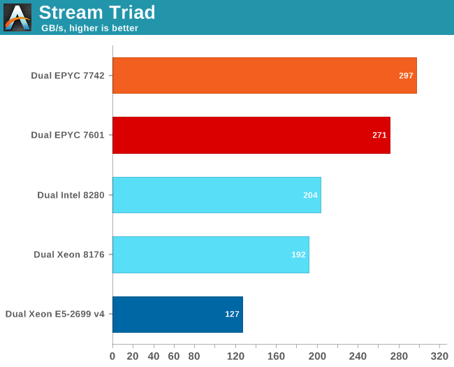
AMD can reach even higher numbers with the setting "number of nodes per socket" (NPS) set to 4. With 4 nodes per socket, AMD reports up to 353 GB/s. NPS4 will cause the CCX to only access the memory controllers with the lowest latency at the central IO Hub chip.
Those numbers only matter to a small niche of carefully AVX(-256/512) optimized HPC applications. AMD claims a 45% advantage compared to the best (28-core) Intel SKUs. We have every reason to believe them but it is only relevant to a niche.
For the rest of the enterprise world (probably 95+%), memory latency has much larger impact than peak bandwidth.


180 Comments
View All Comments
ET - Thursday, August 8, 2019 - link
I found the EPYC 7262 the most interesting SKU. By L3 cache size, that would be 4 chiplets, each offering only 2 cores. From the specs it looks like AMD has no shortage of 4 core chiplets, but I didn't expect 2 core chiplets.Rudde - Friday, August 9, 2019 - link
L3 cache is shared inside a CCX (4 cores), which suggests that every CCX has only one core available, but 16MB of L3 cache. I.e. every core has private L3 cache.colonelclaw - Thursday, August 8, 2019 - link
But can it serve Crysis Battle Royale?shing3232 - Thursday, August 8, 2019 - link
I am pretty sure it can lolBigMamaInHouse - Thursday, August 8, 2019 - link
@ Johan De Gelas will u test @240W TDP config?JohanAnandtech - Thursday, August 8, 2019 - link
Elaborate your interest in that, as it is only tad higher than the official 225W TDP?BigMamaInHouse - Thursday, August 8, 2019 - link
AMD is offering 225W/240W TDP option in bios to it's customers and lets them to decide if to go with better cooling and use 240W or stay at 225W, even though it looks small increase- in reality it should offer almost 10% more power headroom to the CPU chiplets -if you consider that the 225W is including ~55W for I/O die, so extra 15W for the chiplets alone should offer nice bump in clocks.Gondalf - Thursday, August 8, 2019 - link
Strange.....the article forgot Cooper Lake, out in Q4 this year and at major customers (for revenue) from at least two quarters. Same applies to Ice Lake SP that is in evaluation to OEMs right now.From the article looks like Intel is sleeping, but it is not at all. Ummm maybe Intel is snobbing some guys here not giving samples to test?? or informations to share??
Bet Intel have to argue about the test suite or about compiler settings.........
JohanAnandtech - Thursday, August 8, 2019 - link
Because Cooper Lake is still "warmed up Skylake" (unless I missed something). AFAIK it is Cascade Lake with 8 mem channels - so the 56-core socketed will probably be still in the 350-400W TDP range. So the SPEC benchmarks will look better, but getting that kind of server running inside your datacenter does not look very attractive: complex and thus expensive boards, high cooling and power distribution required. Looks like a chip that wins back benchmarks, but is too much hassle to roll out in high quantities.Null666666 - Friday, August 9, 2019 - link
Wondering when 4-8 socket ice lake is due.