AMD Zen 2 Microarchitecture Analysis: Ryzen 3000 and EPYC Rome
by Dr. Ian Cutress on June 10, 2019 7:22 PM EST- Posted in
- CPUs
- AMD
- Ryzen
- EPYC
- Infinity Fabric
- PCIe 4.0
- Zen 2
- Rome
- Ryzen 3000
- Ryzen 3rd Gen
AMD Zen 2 Microarchitecture Overview
The Quick Analysis
At AMD’s Tech Day, on hand was Fellow and Chief Architect Mike Clark to go through the changes. Mike is a great engineer to talk to, although what always amuses me (for any company, not just AMD) is that engineers that talk about the latest products coming to market are already working one, two, or three generations ahead at the company. Mike remarked that it took him a while to think back to the specific Zen+ to Zen 2 changes, while his mind internally is already several generations down the line.
An interesting element to Zen 2 is around the intention. Initially Zen 2 was merely going to be a die shrink of Zen+, going from 12nm down to 7nm, similar to what we used to see with Intel in its tick-tock model for the initial part of the century. However, based on internal analysis and the time frame for 7nm, it was decided that Zen 2 would be used as a platform for better performance, taking advantage of 7nm in multiple ways rather than just redesigning the same layout on a new process node. As a result of the adjustments, AMD is promoting a +15% IPC improvement for Zen 2 over Zen+.
When it comes down to the exact changes in the microarchitecture, what we’re fundamentally looking at is still a similar floorplan to what Zen looks like. Zen 2 is a family member of the Zen family, and not a complete redesign or different paradigm on how to process x86 – as will other architectures that have familial updates, Zen 2 affords a more efficient core and a wider core, allowing better instruction throughput.
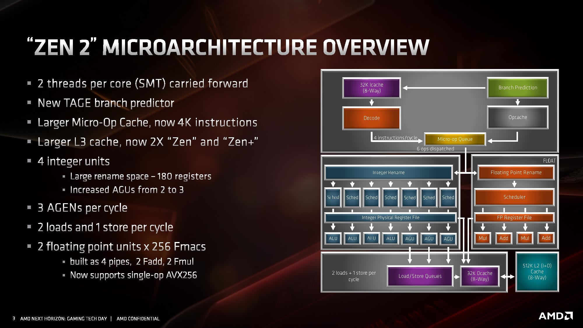
At a high level, the core looks very much the same. Highlights of the Zen 2 design include a different L2 branch predictor known as a TAGE predictor, a doubling of the micro-op cache, a doubling of the L3 cache, an increase in integer resources, an increase in load/store resources, and support for single-operation AVX-256 (or AVX2). AMD has stated that there is no frequency penalty for AVX2, based on its energy aware frequency platform.
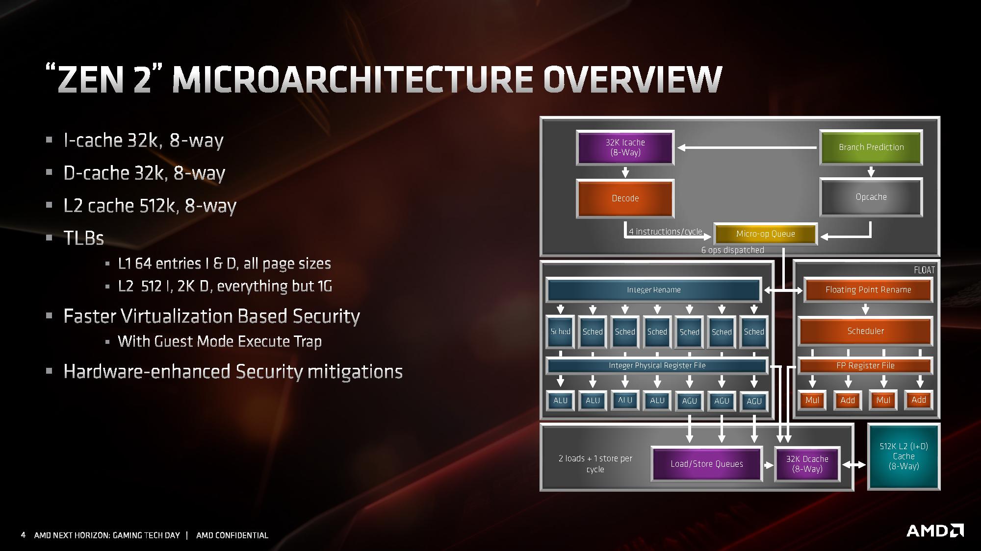
AMD has also made adjustments to the cache system, the most notable being for the L1 instruction cache, which has been halved to 32 kB, but associativity has doubled. This change was made for important reasons, which we’ll go into over the next pages. The L1 data cache and L2 caches are unchanged, however the translation lookaside buffers (TLBs) have increased support. AMD also states that it has added deeper virtualization support with respect to security, helping enable features further down the pipeline. As mentioned previously in this article, there are also security hardening updates.
For the quick analysis, it’s easy to tell that doubling the micro-op cache is going to offer a significant improvement to IPC in a number of scenarios, and combine that with an increase in load/store resources is going to help more instructions get pushed through. The double L3 cache is going to help in specific workloads, as would the AVX2 single-op support, but the improved branch predictor is also going to showcase raw performance uplift. All-in-all, for an on-paper analysis, AMD’s +15% IPC improvement seems like a very reasonable number to promote.
Over the next few pages, we’ll go deeper into how the microarchitecture has changed.


216 Comments
View All Comments
nandnandnand - Tuesday, June 11, 2019 - link
Shouldn't we be looking at highest transistors per square millimeter plotted over time? The Wikipedia article helpfully includes die area for most of the processors, but the graph near the top just plots number of transistors without regard to die size. If Intel's Xe hype is accurate, they will be putting out massive GPUs (1600 mm^2?) made of multiple connected dies, and AMD already does something similar with CPU chiplets.I know that the original Moore's law did not take into account die size, multi chip modules, etc. but to ignore that seems cheaty now. Regardless, performance is what really matters. Hopefully we see tight integration of CPU and L4 DRAM cache boosting performance within the next 2-3 years.
Wilco1 - Wednesday, June 12, 2019 - link
Moore's law is about transistors on a single integrated chip. But yes density matters too, especially actual density achieved in real chips (rather than marketing slides). TSMC 7nm does 80-90 million transistors/mm^2 for A12X, Kirin 980, Snapdragon 8cx. Intel is still stuck at ~16 million transistors/mm^2.FunBunny2 - Wednesday, June 12, 2019 - link
enough about Moore, unless you can get it right. Moore said nothing about transistors. He said that compute capability was doubling about every second year. This is what he actually wrote:"The complexity for minimum component costs has increased at a rate of roughly a factor of two per year. Certainly over the short term this rate can be expected to continue, if not to increase. Over the longer term, the rate of increase is a bit more uncertain, although there is no reason to believe it will not remain nearly constant for at least 10 years. "
[the wiki]
the main reason the Law has slowed is just physics: Xnm is little more (teehee) than propaganda for some years, at least since the end of agreed dimensions of what a 'transistor' was. couple that with the coalescing of the maths around 'the best' compute algorithms; complexity has run into the limiting factor of the maths. you can see it in these comments: gimme more ST, I don't care about cores. and so on. Mother Nature's Laws are fixed and immutable; we just don't know all of them at any given moment, but we're getting closer. in the old days, we had the saying 'doing the easy 80%'. we're well into the tough 20%.
extide - Monday, June 17, 2019 - link
"The complexity for minimum component costs..."He was directly referring to transistor count with the word "complexity" in your quote -- so yes he was literally talking about transistor count.
crazy_crank - Tuesday, June 11, 2019 - link
Actually the number of cores doesn't matter AFAIK, as Moores Law originally only was about transistor density, so all you need to compare is transistors per square millimeter. Looked at it like this, it actually doesn't even look that badchada - Wednesday, June 12, 2019 - link
Moore's law specifically talks about density doubling. If they can fit 6 cores into the same footprint, you can absolutely consider 6 cores for a density comparison. That being said, we have been off this pace for a while.III-V - Wednesday, June 12, 2019 - link
>Moore's law specifically talks about density doubling.No it doesn't.
Jesus Christ, why is Moore's Law so fucking hard for people to understand?
LordSojar - Thursday, June 13, 2019 - link
Why it ever became known as a "law" is totally beyond me. More like Moore's Theory (and that's pushing it, as he made a LOT of suppositions about things he couldn't possibly predict, not being an expert in those areas. ie material sciences, quantum mechanics, etc)sing_electric - Friday, June 14, 2019 - link
This. He wasn't describing something fundamental about the way nature works - he was looking at technological advancements in one field over a short time frame. I guess 'Moore's Observation" just didn't sound as good.And the reason why no one seems to get it right is that Moore wrote and said several different things about it over the years - he'd OBSERVED that the number of transistors you could get on an IC was increasing at a certain rate, and from there, that this lead to performance increases, so both the density AND performance arguments have some amount of accuracy behind them.
And almost no one points out that it's ultimately just a function of geometry: As process decreases linearly (say, 10 units to 7 units) , you get a geometric increase in the # of transistors because you get to multiply that by two dimensions. Other benefits - like decreased power use per transistor, etc. - ultimately flow largely from that as well (or they did, before we had to start using more and more exotic materials to get shrinks to work.)
FunBunny2 - Thursday, June 13, 2019 - link
"Jesus Christ, why is Moore's Law so fucking hard for people to understand?"because, in this era of truthiness, simplistic is more fun than reality. Moore made his observation in 1965, at which time IC fabrication had not even reached LSI levels. IOW, the era when node size was dropping like a stone and frequency was rising like a Saturn rocket; performance increases with each new iteration of a device were obvious to even the most casual observer. just like prices in the housing market before the Great Recession, the simpleminded still think that both vectors will continue forevvvvaaahhh.