AMD Zen 2 Microarchitecture Analysis: Ryzen 3000 and EPYC Rome
by Dr. Ian Cutress on June 10, 2019 7:22 PM EST- Posted in
- CPUs
- AMD
- Ryzen
- EPYC
- Infinity Fabric
- PCIe 4.0
- Zen 2
- Rome
- Ryzen 3000
- Ryzen 3rd Gen
Integer Units, Load and Store
The integer unit schedulers can accept up to six micro-ops per cycle, which feed into the 224-entry reorder buffer (up from 192). The Integer unit technically has seven execution ports, comprised of four ALUs (arithmetic logic units) and three AGUs (address generation units).
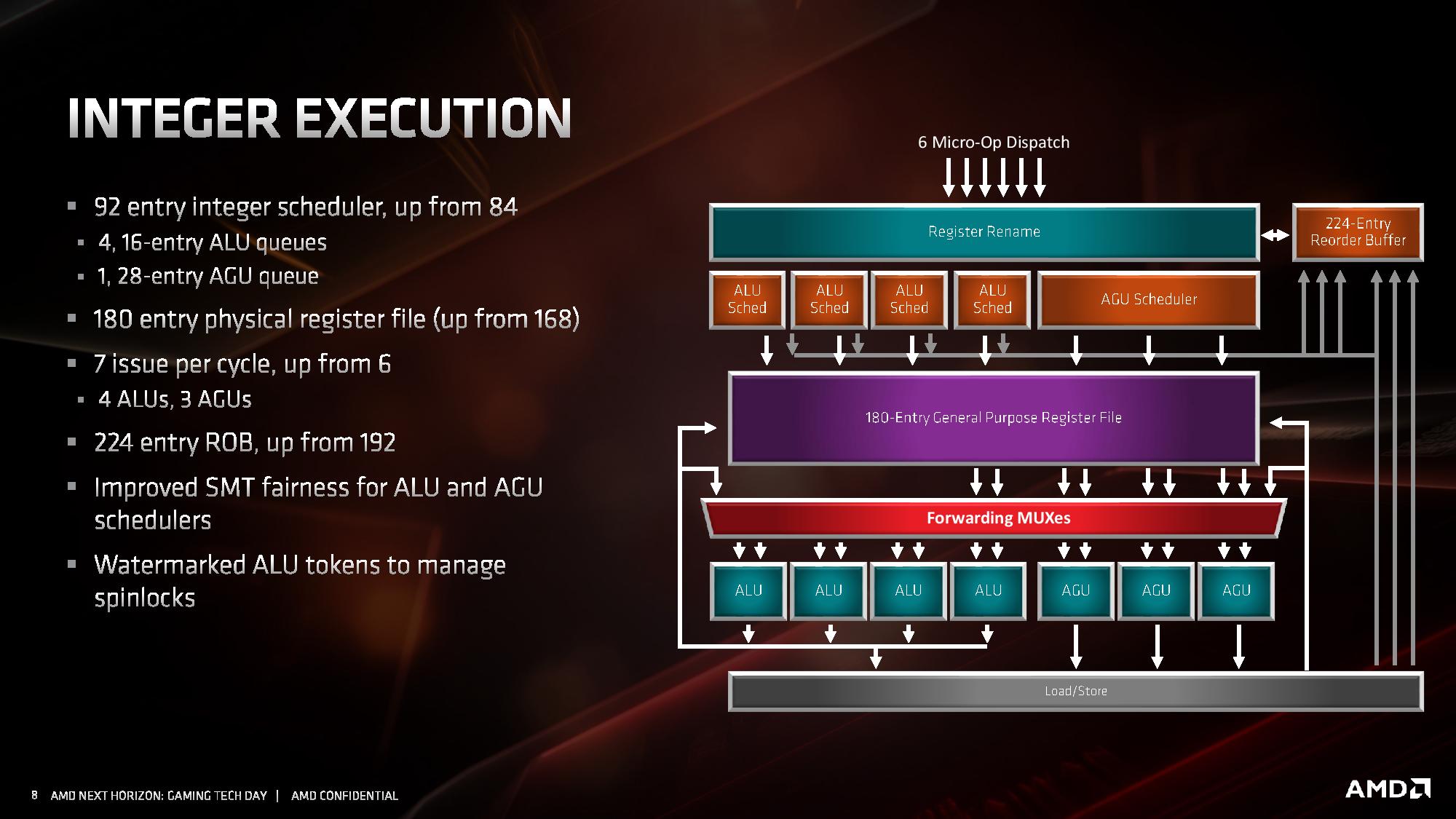
The schedulers comprise of four 16-entry ALU queues and one 28-entry AGU queue, although the AGU unit can feed 3 micro-ops per cycle into the register file. The AGU queue has increased in size based on AMD’s simulations of instruction distributions in common software. These queues feed into the 180-entry general purpose register file (up from 168), but also keep track of specific ALU operations to prevent potential halting operations.
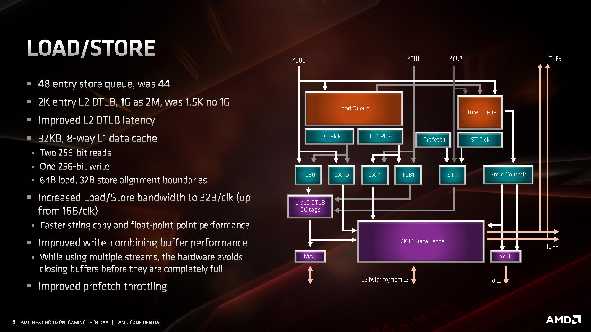
The three AGUs feed into the load/store unit that can support two 256-bit reads and one 256-bit write per cycle. Not all the three AGUs are equal, judging by the diagram above: AGU2 can only manage stores, whereas AGU0 and AGU1 can do both loads and stores.
The store queue has increased from 44 to 48 entries, and the TLBs for the data cache have also increased. The key metric here though is the load/store bandwidth, as the core can now support 32 bytes per clock, up from 16.


216 Comments
View All Comments
mikato - Tuesday, June 11, 2019 - link
Hehe, yeah I saw that. That was a good one for the marketing team or whoever makes the slides.Atari2600 - Wednesday, June 12, 2019 - link
No, for each of those line items they should have said "Intel only"zalves - Tuesday, June 11, 2019 - link
I really don't understand how one can compare these AMD CPU's with Intel's HEDT, they lack PCIe Lanes and don't support quad-channel memory. And that a huge deal breaker for anyone that wants and needs some serious IO and multi tasking.TheUnhandledException - Tuesday, June 11, 2019 - link
Well that is what Threadripper is for. Can't wait to see the 3000 series Threadrippers.John_M - Tuesday, June 11, 2019 - link
So, 5th generation EPYC codename is going to be either Turin, Bolognia or Florence as Palermo has already been used for Sempron.John_M - Tuesday, June 11, 2019 - link
*that's Bologna, of course. It would be nice to be able to edit posts for typos.WaltC - Tuesday, June 11, 2019 - link
Great read!John_M - Tuesday, June 11, 2019 - link
What is the advantage in halving the L1 instruction cache? Was the change forced by the doubling of its associativity? According to the (I suspect somewhat oversimplified) Wikipedia article on CPU Cache, doubling the associativity increases the probability of a hit by about the same amount as doubling the cache size, but with more complexity. So how is this Zen2 configuration better than that in Zen and Zen+?John_M - Tuesday, June 11, 2019 - link
Ah! It's sort of explained at the bottom of page 7. I had glossed over that because the first two paragraphs were too technical for my understanding. I see that it was halved to make room for something else to be made bigger, which on balance seems to be a successful trade off.arnd - Wednesday, June 12, 2019 - link
More importantly, 32K 8-way is a sweet spot for an L1 cache. This is what AMD is using for the D$ already and what all modern Intel L1 caches (both I and D) are. With eight ways, this is the largest size you can have for a non-aliasing virtually indexed cache using the 4KB page size of the x86 architecture. Having more than eight ways has diminishing returns, so going beyond 32KB requires extra complexity for dealing with aliasing or physically indexed caches like the L2.