AMD Zen 2 Microarchitecture Analysis: Ryzen 3000 and EPYC Rome
by Dr. Ian Cutress on June 10, 2019 7:22 PM EST- Posted in
- CPUs
- AMD
- Ryzen
- EPYC
- Infinity Fabric
- PCIe 4.0
- Zen 2
- Rome
- Ryzen 3000
- Ryzen 3rd Gen
AMD Zen 2 Microarchitecture Overview
The Quick Analysis
At AMD’s Tech Day, on hand was Fellow and Chief Architect Mike Clark to go through the changes. Mike is a great engineer to talk to, although what always amuses me (for any company, not just AMD) is that engineers that talk about the latest products coming to market are already working one, two, or three generations ahead at the company. Mike remarked that it took him a while to think back to the specific Zen+ to Zen 2 changes, while his mind internally is already several generations down the line.
An interesting element to Zen 2 is around the intention. Initially Zen 2 was merely going to be a die shrink of Zen+, going from 12nm down to 7nm, similar to what we used to see with Intel in its tick-tock model for the initial part of the century. However, based on internal analysis and the time frame for 7nm, it was decided that Zen 2 would be used as a platform for better performance, taking advantage of 7nm in multiple ways rather than just redesigning the same layout on a new process node. As a result of the adjustments, AMD is promoting a +15% IPC improvement for Zen 2 over Zen+.
When it comes down to the exact changes in the microarchitecture, what we’re fundamentally looking at is still a similar floorplan to what Zen looks like. Zen 2 is a family member of the Zen family, and not a complete redesign or different paradigm on how to process x86 – as will other architectures that have familial updates, Zen 2 affords a more efficient core and a wider core, allowing better instruction throughput.
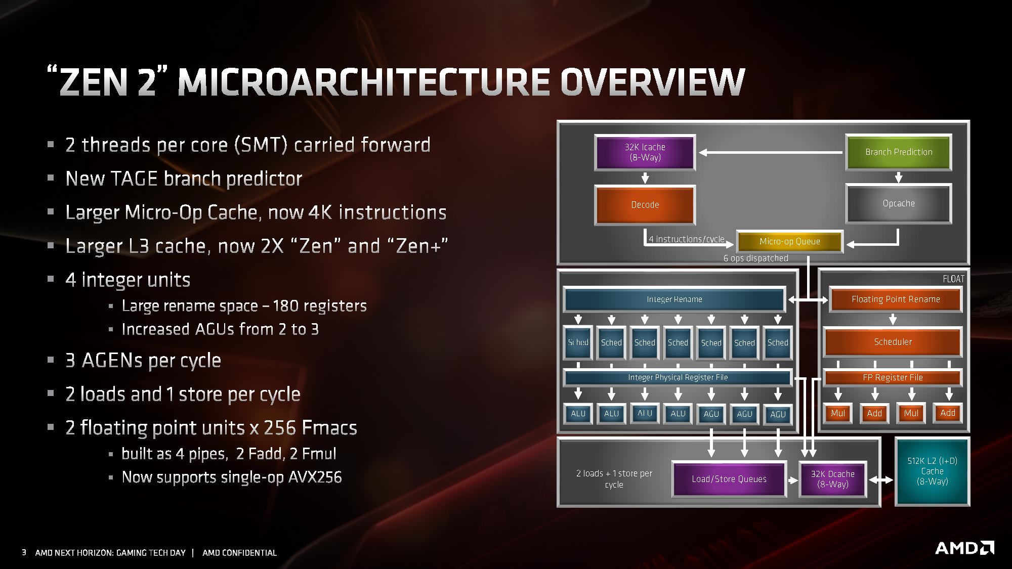
At a high level, the core looks very much the same. Highlights of the Zen 2 design include a different L2 branch predictor known as a TAGE predictor, a doubling of the micro-op cache, a doubling of the L3 cache, an increase in integer resources, an increase in load/store resources, and support for single-operation AVX-256 (or AVX2). AMD has stated that there is no frequency penalty for AVX2, based on its energy aware frequency platform.
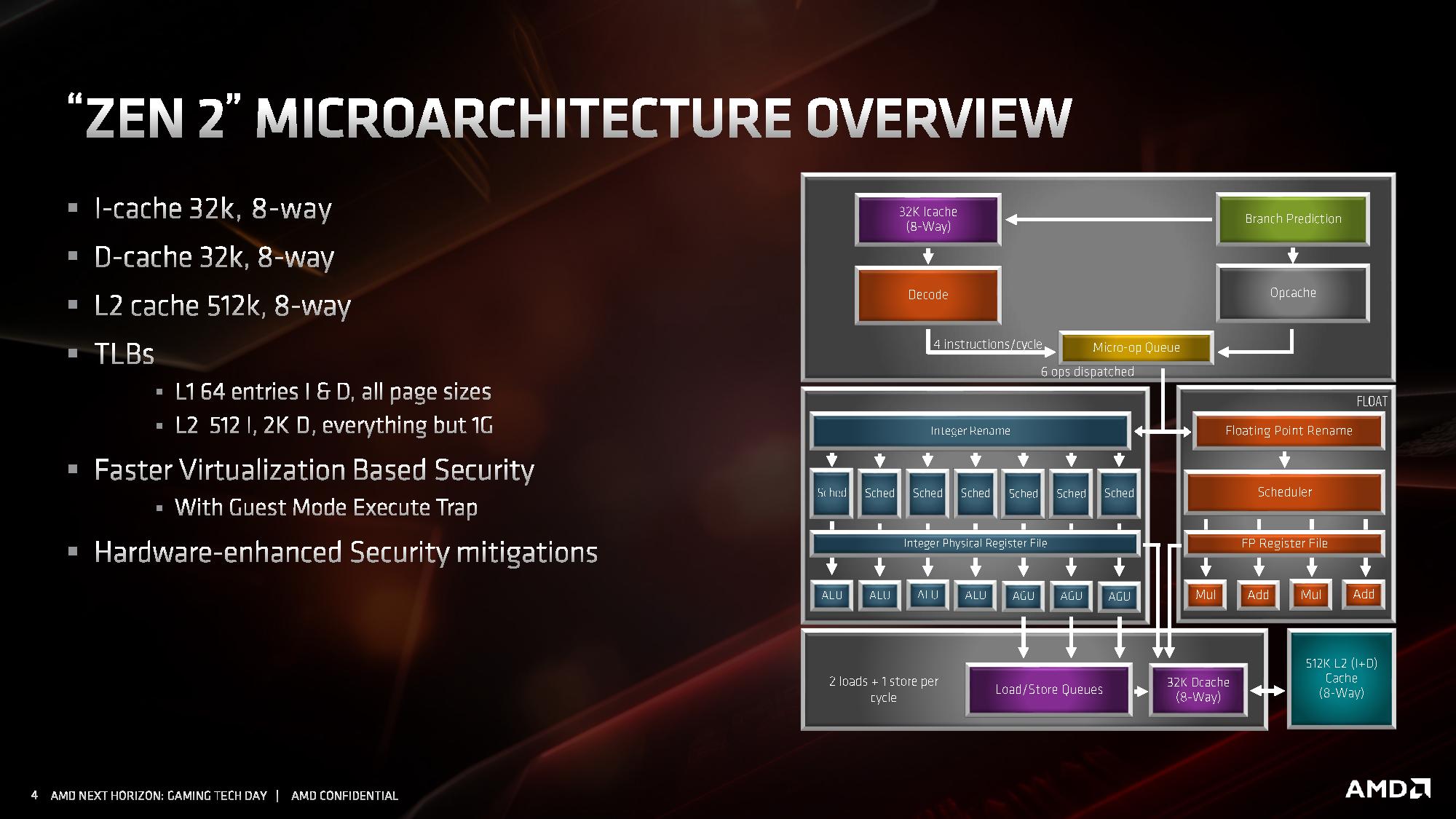
AMD has also made adjustments to the cache system, the most notable being for the L1 instruction cache, which has been halved to 32 kB, but associativity has doubled. This change was made for important reasons, which we’ll go into over the next pages. The L1 data cache and L2 caches are unchanged, however the translation lookaside buffers (TLBs) have increased support. AMD also states that it has added deeper virtualization support with respect to security, helping enable features further down the pipeline. As mentioned previously in this article, there are also security hardening updates.
For the quick analysis, it’s easy to tell that doubling the micro-op cache is going to offer a significant improvement to IPC in a number of scenarios, and combine that with an increase in load/store resources is going to help more instructions get pushed through. The double L3 cache is going to help in specific workloads, as would the AVX2 single-op support, but the improved branch predictor is also going to showcase raw performance uplift. All-in-all, for an on-paper analysis, AMD’s +15% IPC improvement seems like a very reasonable number to promote.
Over the next few pages, we’ll go deeper into how the microarchitecture has changed.


216 Comments
View All Comments
The_Assimilator - Wednesday, June 12, 2019 - link
The original version of this article noted the 3950X price wasn't confirmed at the time of publication, but it seems they edited that bit out after Su's presentation.Still need the table to be updated - PCIe and DDR4 columns at least.
vFunct - Tuesday, June 11, 2019 - link
Eventually these Multi-chip packages should incorporate system DRAM (via HBM) as well as SSD NVRAM and GPUs, and sold as full packages that you'd typically see in common configurations. 64GB memory + 1TB SSD + 16 CPU cores + whatever GPU.mode_13h - Tuesday, June 11, 2019 - link
GPUs are often upgraded more often than CPUs. And GPUs dissipate up to about 300 W, while desktop CPUs often around 100 W (except for Intel's Coffee Lake).So, it wouldn't really seem like CPUs and GPUs belong together, either from an upgrade or a cooling perspective. Consoles can make it work by virtue of being custom form factor and obviously you don't upgrade a console's GPU or CPU - you just buy a new console.
Therefore, I don't see this grand unification happening for performance-oriented desktops. That said, APUs will probably continue to get more powerful and perhaps occupy ever more of the laptop market.
Threska - Tuesday, June 11, 2019 - link
I imagine that's why there's PCIe 4.0 and now 5.0.R3MF - Tuesday, June 11, 2019 - link
memory support?3200 official, or higher...
SquarePeg - Tuesday, June 11, 2019 - link
According to AMD 3200mhz is officially supported but they (AMD) have had memory clocked to over 5000mhz. Infinity fabric will run 1:1 with up to 3733mhz ram but any higher and it splits to 2:1. AMD also said that they have found DDR4 3600 16-21-21 to be the best bang for buck on performance returns.R3MF - Wednesday, June 12, 2019 - link
cheersGastec - Wednesday, June 12, 2019 - link
But will those be 3200 MHz overclocked (XMP) or 3200 SPD?Cooe - Wednesday, June 12, 2019 - link
The latter. Only >3200MHz is now overclocked.Lord of the Bored - Tuesday, June 11, 2019 - link
That security slide, though...Most of a page of "N/A"
I love it.