Examining Intel's Ice Lake Processors: Taking a Bite of the Sunny Cove Microarchitecture
by Dr. Ian Cutress on July 30, 2019 9:30 AM EST- Posted in
- CPUs
- Intel
- 10nm
- Microarchitecture
- Ice Lake
- Project Athena
- Sunny Cove
- Gen11
Gen11 Graphics: Competing for 1080p Gaming
The new message from Intel is that it is driving to deliver deep gaming experiences with its technology, and the nod to the future is specifically what it wants to do with its graphics technology. Until the company is ready with its Xe designs for 2020 and beyond, it wants to start to lead the way with better integrated designs. That starts with Ice Lake, where the most powerful version of Ice Lake will offer over 1TF of compute performance, support higher resolution HEVC, better display pipes, an enhanced rasterizer, and support for Adaptive Sync.
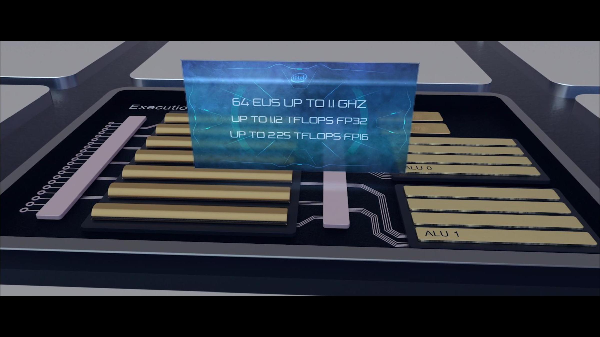
The key words in that last sentence were ‘the most powerful version’. Because Intel hasn’t really spoken about its product stack yet, the company has been leading with its most powerful Iris Plus designs. We assume this means 28W? That means its high-end performance products, in the best designs, with the fastest memory. Compared to the standard Gen9 implementation of 24 execution units at 1150 MHz turbo, the best Ice Lake Gen11 design will deliver 64 execution units up to a 1100 MHz frequency, good for 1.15 TF of FP32 performance, or 2.30 TF of FP16 performance. Intel promise up to 1.8x better frame rates in games with the best Ice Lake compared to an average 8th Gen Core (Kaby Lake) Gen9 implementation. Intel doesn’t compare the results to a hypothetical Cannon Lake Gen10 implementation.
Intel hasn’t stated how many graphics configurations it will offer, but there would appear to be several given what information has leaked out already. The high-end design with 64 execution units will be called Iris Plus, but there will be a ‘UHD’ version for mid-range and low-end parts, however Intel has not stated how many execution units these parts will have. We suspect that standard dividers will be in play, with 24/32/48 EU designs possible as different parts of the GPU are fused off. There may be some potential for increased frequency in these designs, reducing latency, but ultimately reduced performance over the top design.
It should be noted that Intel is promoting the top model as being suitable for 1080p low-to-mid gaming, which would imply that models with fewer execution units may struggle to hit those highs with different EU counts. Until Intel gives us a full and proper product list, it is hard to tell at this point.
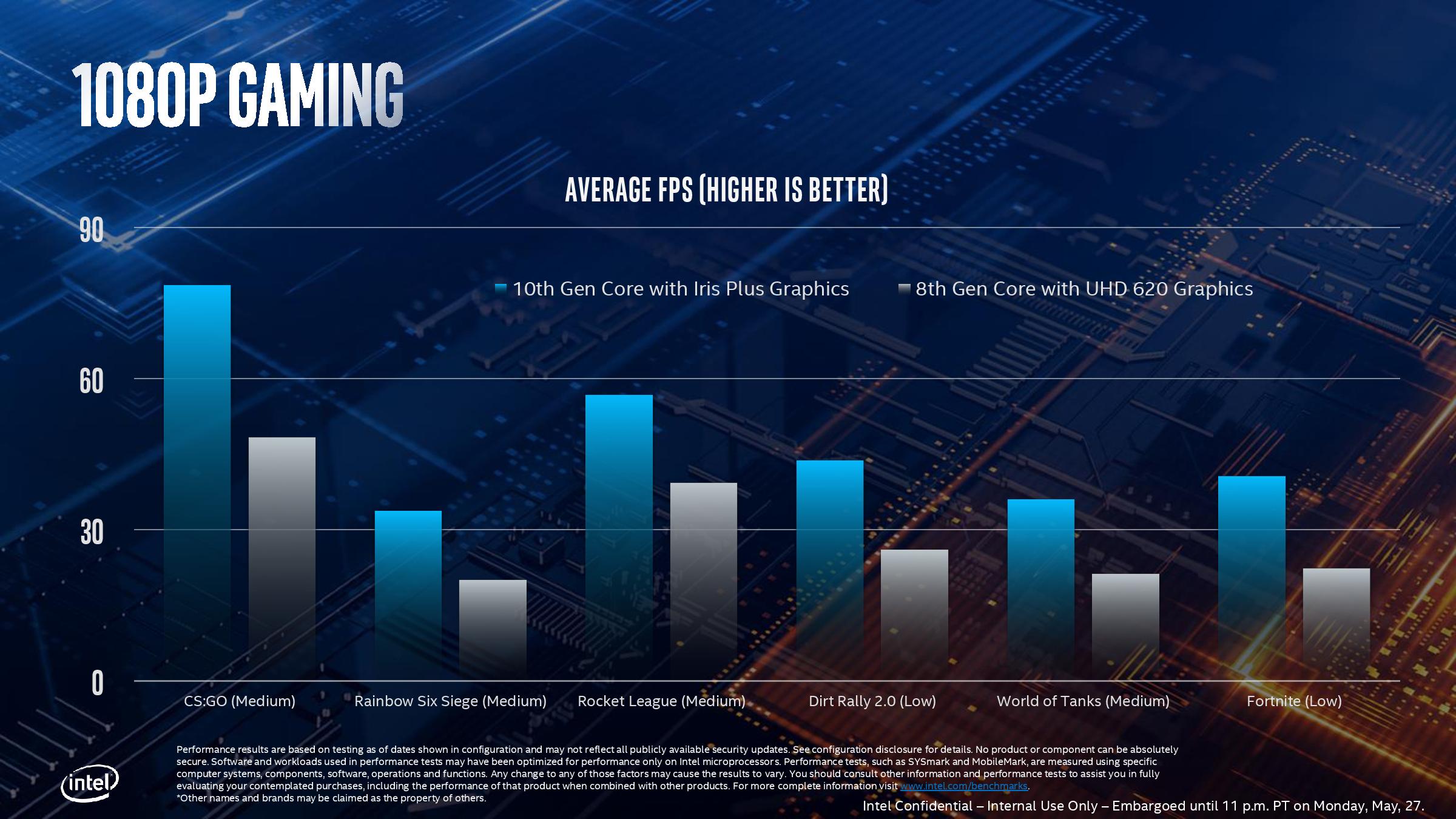
This slide, for example, shows where Intel expects its highest Ice Lake implementation to perform compared to the standard 8th Gen solution. As part of Computex, Intel also showed off some different data:
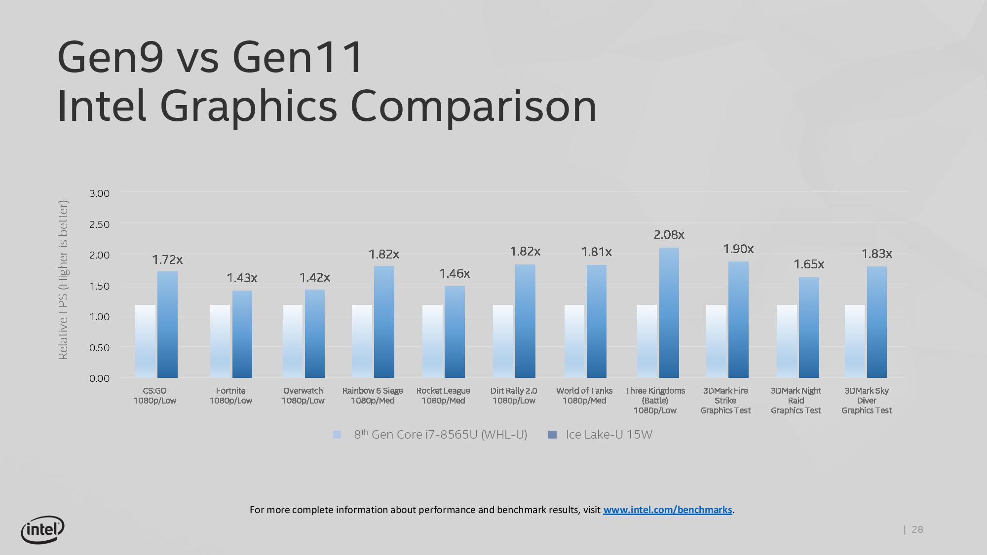
This graph shows relative FPS, rather than actual FPS, so it’s hard to see if certain games are just hitting 30 FPS in the highest mode. The results here are a function of the combination of increased EU count but also memory bandwidth.
Features for All
There are a number of features that all of the Gen11 graphics implementations will get, regardless of its number of execution units.
For its fixed function units, Gen11 supports two HEVC 10-bit encode pipelines, either two 4K60 4:4:4 streams simultaneously or one 8K30 4:2:2 stream using both pipelines at once. On display pipes, Gen11 has access to three 4K pipes split between DP1.4 HBR3 and HDMI 2.0b. There is also support for 2x 5K60 or 1x 4K120 with a 10-bit color depth.
The rasterizer gets an upgrade, and will now do 16 pixels per clock or 32 bilinear filtered texels per clock. Intel also gives some insight into the cache arrangements, with the execution units having their own 3 MiB of L3 cache and 0.5 MiB of shared local memory.
Intel recommends that to get the best out of the graphics, it should be paired with LPDDR4X-3733 memory in order to extract a healthy 50-60 GB/s bandwidth, and we should expect a number of Project Athena approved designs do just that. However, at the lower end of Ice Lake devices, we might see single channel DDR4 designs take over due to costs, which might limit performance. As always for integrated graphics, memory bandwidth is often a major bottleneck in performance. Back when Intel had eDRAM enabled Crystalwell designs, those chips were good for 50 GB/s bidirectional bandwidth, and we are almost at that stage with DRAM bandwidth designs now. It should be noted that there are tradeoffs with memory support: LPDDR4/X supports 4x 32b channels up to 32 GB with super low power consumption modes, but if users want more capacity, they’ll have to look to DDR4-3200 with 2x 64b channels up to 64 GB, but lose some performance and power savings.
Variable Rate Shading
A feature being implemented in Gen11 is Variable Rate Shading. VRS is a game-dependent technology that allows the GPU adjust the shading performance of the scene render based on what areas are important. All games currently do shading on a per-pixel basis, meaning that each pixel has a full calculation and that data is transferred to the final image. With VRS, shading is calculated over several pixels at once – essentially doing pixel shading in a coarser, lower-resolution manner – to save post-processing time by using averaged data.
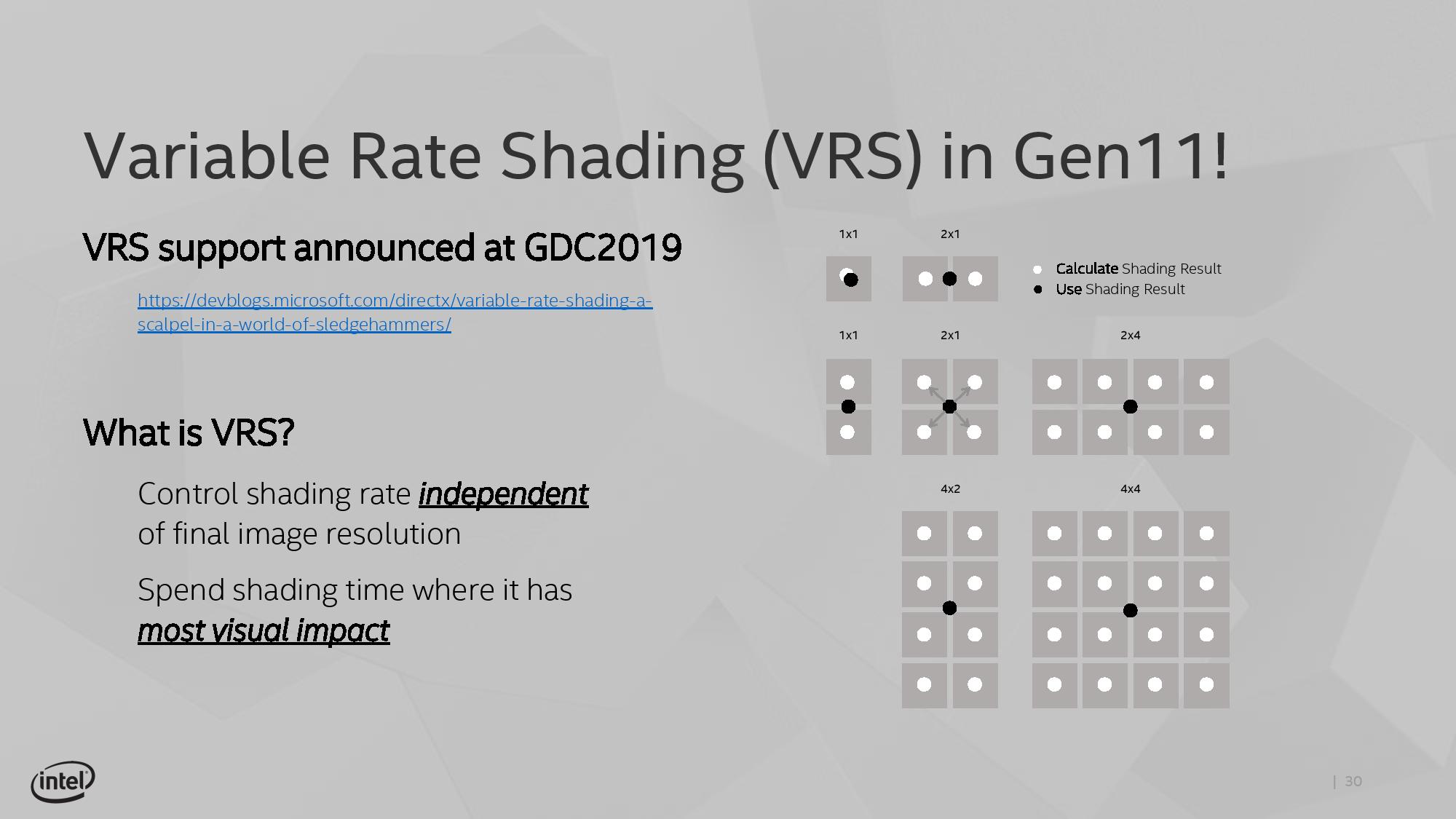
The idea is that using this method can reduce some of the load on the execution units, ultimately increasing the frame rate. The size of that combination of pixels can be adjusted on a per-frame basis as well, allowing the game to take advantage of processing budget where it exists, or pull back to a point where performance is needed. Ultimately Intel believes that any image quality loss is not noticeable, especially for the performance impact they expect it to provide. Intel states that this technology is useful for areas such as lighting adjustments, partially obscured objects (by fog/clouds), and areas that undergo blur, or foveated rendering – basically any area where clarity isn’t explicitly required to begin with.
The only issue here though is an ecosystem one – it requires the game developer support. Intel is already working with Epic to add it to the Unreal Engine, and Intel has worked with developers to enable support in titles such as Civilization 6. The difference in performance, according to Intel, can be up to a 30% FPS increase in a best-case scenario. NVIDIA already supports VRS through dedicated hardware, whereas AMD’s current solutions are best described as a more limited shader-based approximation.


107 Comments
View All Comments
repoman27 - Tuesday, July 30, 2019 - link
"It stands to reason then that the smaller package is for lower performance and low power options, despite being exactly the same silicon."I know the die floorplans are the same, but have Intel ever actually confirmed that U and Y (or H and S series for that matter) are the exact same silicon? Is it strictly binning and packaging that separates the platforms, or is there a slight tweak to the manufacturing process to target lower power / higher frequencies? Intel production roadmaps would seem to indicate this isn't just a binning situation, but I've never been entirely certain on that point.
And isn't Comet Lake-U 6+2 more likely to be 25 W, with Whiskey Lake-U 4+2 continuing to pull 15 W duty alongside Ice Lake-U 4+2?
CaedenV - Tuesday, July 30, 2019 - link
Those goals for Aethena are OK, but my old Dell XPS 12 with a carousel frame hit all of those except biometric, and wake from sleep in <1 sec... well, and the bezel... but that was due to the carousel design which I would LOVE to come back in a more modern form.Not saying these goals are bad... but if a 6 year old midrange laptop can hit almost all of them, then this isn't exactly aiming for something amazing.
AshlayW - Tuesday, July 30, 2019 - link
Quad core for 179 USD? What is this, 2015? No thanks.HStewart - Tuesday, July 30, 2019 - link
You do realize these are ultra-portable low power cpu's and not desktop chipsSamus - Tuesday, July 30, 2019 - link
Intel is a mess right now, the execution of this along with the naming scheme is ridiculous.shabby - Tuesday, July 30, 2019 - link
18% ipc gain and 20% clock lossPlace your bets how intel will spin this.
CHADBOGA - Tuesday, July 30, 2019 - link
I'm quite disappointed the issue of security mitigation in hardware was not addressed. o_OCityBlue - Saturday, August 3, 2019 - link
Disappointed, but not surprised.Security (and by inference the performance overhead required to implement proper security) is not important according to Anandtech/Ian Cutress. Which is obvious nonsense, so the only logical conclusion is that Anandtech are now a thoroughly biased outfit incapable of any critical reporting, which is quite sad particularly as it means all their articles (particularly when they relate to Intel) have to be read with a very heavy dose of cynicism.
eek2121 - Wednesday, July 31, 2019 - link
That picture of you biting a wafer is priceless.Santoval - Wednesday, July 31, 2019 - link
If Ice Lake-U has a ~3.5% higher single core performance (and, assuming the "multi-core overhead" is the same, multi-core performance as well) than Whiskey Lake-U despite having a 20% lower single core boost clock, then Sunny Cove must be an extremely impressive μarch. Or, er, that might not actually be the case : Ice Lake-U has a 18% higher IPC than the *original* Skylake of 2015, not Whiskey Lake. While Whiskey Lake is basically the same design it must have a somewhat higher IPC due to its much more mature process node and other optimizations.Let's be conservative and assume that Ice Lake-U (more specifically Sunny Cove) has a nice round 15% higher IPC than Whiskey Lake-U, with both at 15W. In that case, at a 20% lower boost clock Ice Lake-U should have a 5% lower performance than Whiskey Lake-U. Where is that +3.5% performance derived from then?
Even if we assumed that Ice Lake-U 18% IPC edge is over Whiskey Lake-U (highly unlikely, otherwise Intel would not have dug out the original Skylake from its computing grave) that would still translate to Ice Lake-U having a 1.5% lower single core performance than Whiskey Lake-U, rather than being 3.5% faster than it.
Maybe, just maybe, this is why Intel used just a single synthetic benchmark (surely compiled with aggressive flags and optimized for Intel CPUs) for that graph and avoided to disclose other synthetic benchmarks and real world use benchmarks? Is this also why they avoided to talk about CPU performance of Ice Lake in their Computex presentation, and instead focused on iGPU, Wifi and AI performance?
Based on the disclosed clocks and the "disclosed" (in obfuscated form) IPC of Ice Lake-U I just cannot see it being in any way faster than Whiskey Lake-U. It will probably also have worse power efficiency, since it has the same or higher TDP range at a much lower clock.