Examining Intel's Ice Lake Processors: Taking a Bite of the Sunny Cove Microarchitecture
by Dr. Ian Cutress on July 30, 2019 9:30 AM EST- Posted in
- CPUs
- Intel
- 10nm
- Microarchitecture
- Ice Lake
- Project Athena
- Sunny Cove
- Gen11
Gen11 Graphics: Competing for 1080p Gaming
The new message from Intel is that it is driving to deliver deep gaming experiences with its technology, and the nod to the future is specifically what it wants to do with its graphics technology. Until the company is ready with its Xe designs for 2020 and beyond, it wants to start to lead the way with better integrated designs. That starts with Ice Lake, where the most powerful version of Ice Lake will offer over 1TF of compute performance, support higher resolution HEVC, better display pipes, an enhanced rasterizer, and support for Adaptive Sync.
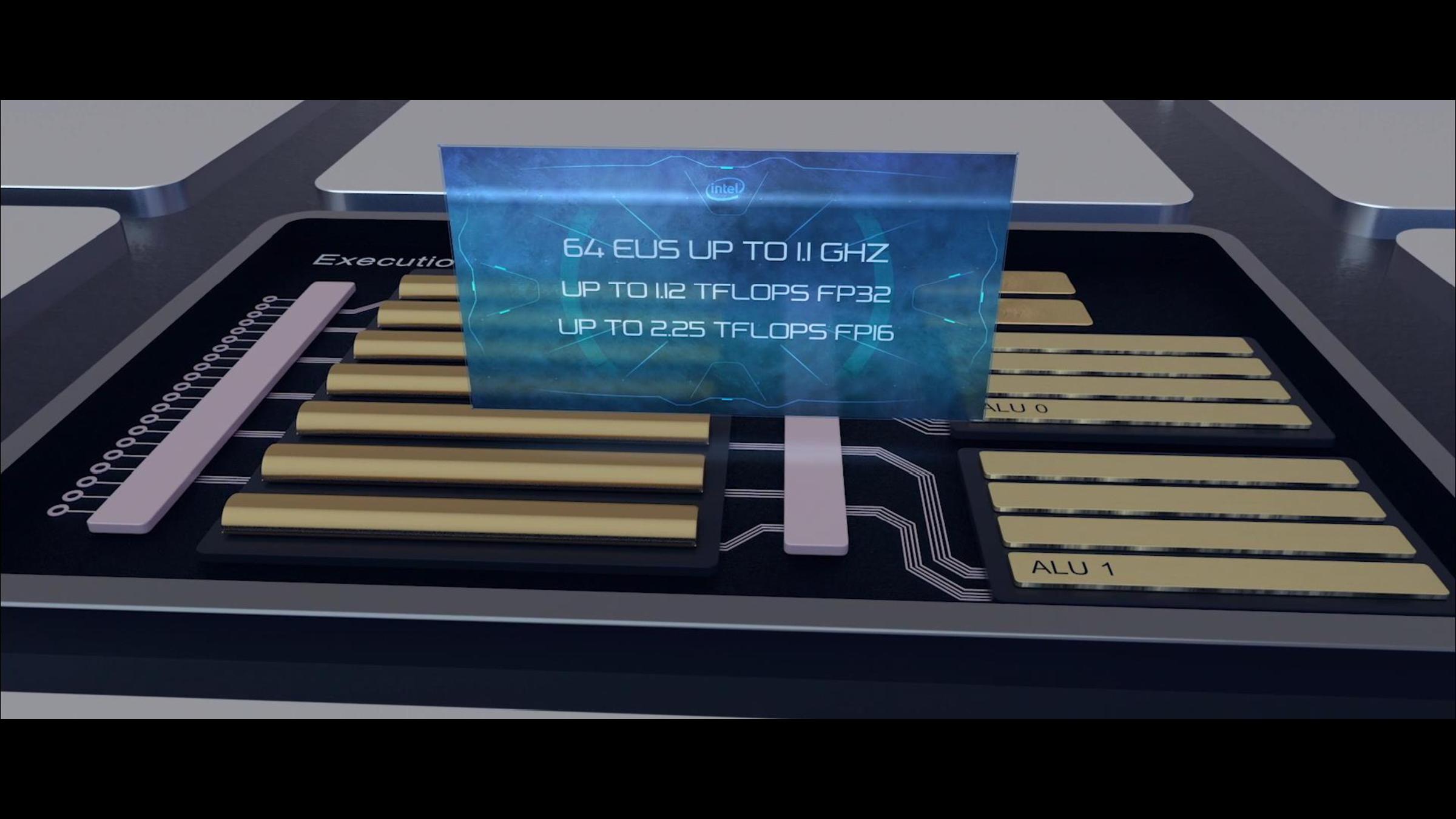
The key words in that last sentence were ‘the most powerful version’. Because Intel hasn’t really spoken about its product stack yet, the company has been leading with its most powerful Iris Plus designs. We assume this means 28W? That means its high-end performance products, in the best designs, with the fastest memory. Compared to the standard Gen9 implementation of 24 execution units at 1150 MHz turbo, the best Ice Lake Gen11 design will deliver 64 execution units up to a 1100 MHz frequency, good for 1.15 TF of FP32 performance, or 2.30 TF of FP16 performance. Intel promise up to 1.8x better frame rates in games with the best Ice Lake compared to an average 8th Gen Core (Kaby Lake) Gen9 implementation. Intel doesn’t compare the results to a hypothetical Cannon Lake Gen10 implementation.
Intel hasn’t stated how many graphics configurations it will offer, but there would appear to be several given what information has leaked out already. The high-end design with 64 execution units will be called Iris Plus, but there will be a ‘UHD’ version for mid-range and low-end parts, however Intel has not stated how many execution units these parts will have. We suspect that standard dividers will be in play, with 24/32/48 EU designs possible as different parts of the GPU are fused off. There may be some potential for increased frequency in these designs, reducing latency, but ultimately reduced performance over the top design.
It should be noted that Intel is promoting the top model as being suitable for 1080p low-to-mid gaming, which would imply that models with fewer execution units may struggle to hit those highs with different EU counts. Until Intel gives us a full and proper product list, it is hard to tell at this point.
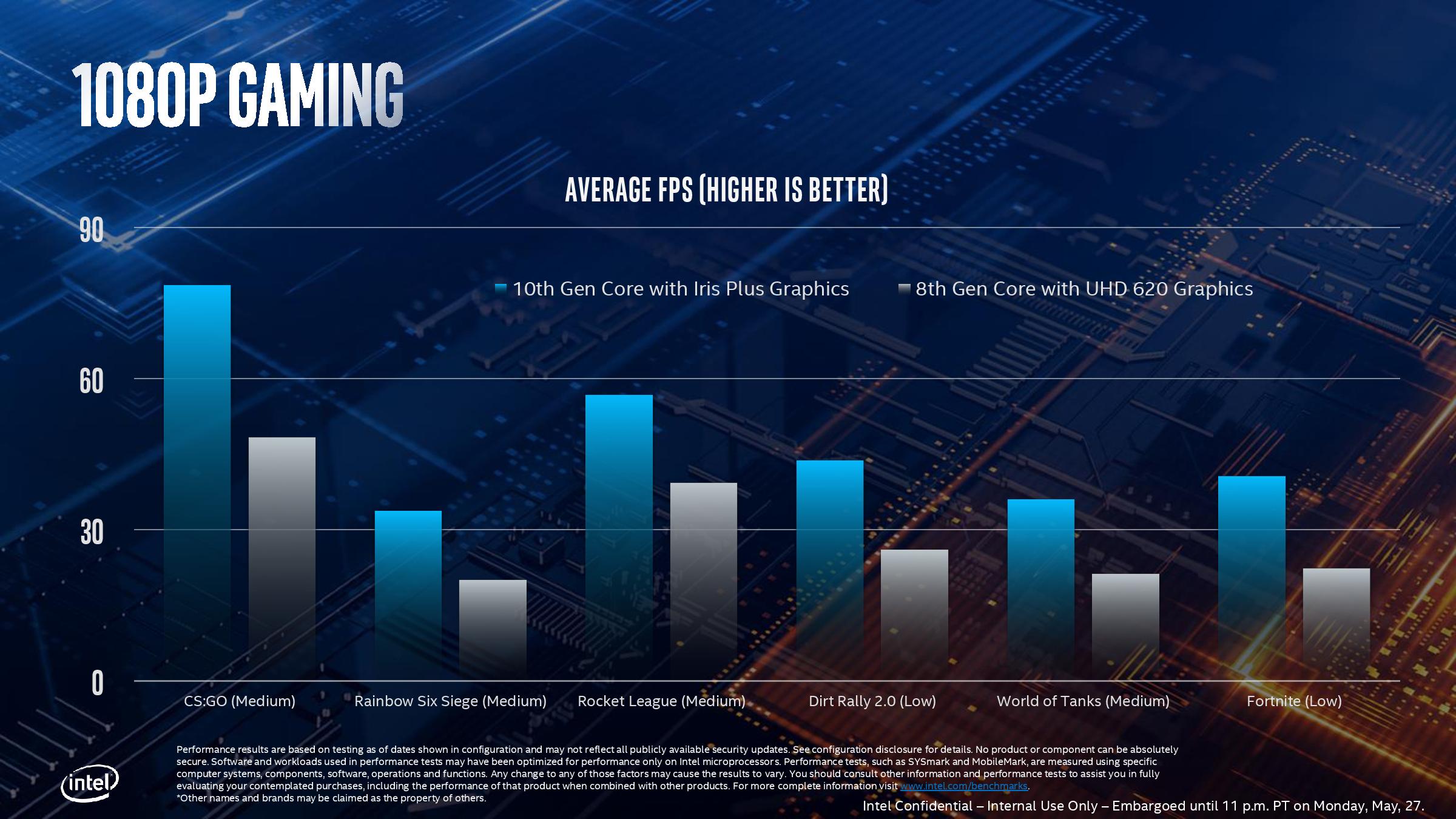
This slide, for example, shows where Intel expects its highest Ice Lake implementation to perform compared to the standard 8th Gen solution. As part of Computex, Intel also showed off some different data:
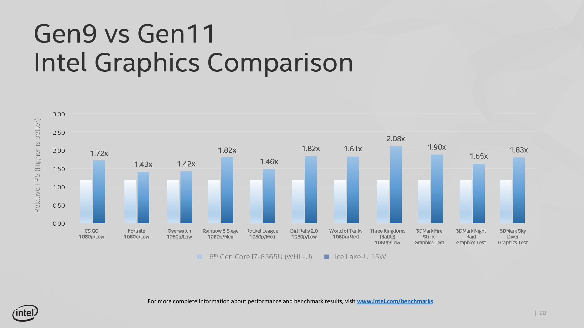
This graph shows relative FPS, rather than actual FPS, so it’s hard to see if certain games are just hitting 30 FPS in the highest mode. The results here are a function of the combination of increased EU count but also memory bandwidth.
Features for All
There are a number of features that all of the Gen11 graphics implementations will get, regardless of its number of execution units.
For its fixed function units, Gen11 supports two HEVC 10-bit encode pipelines, either two 4K60 4:4:4 streams simultaneously or one 8K30 4:2:2 stream using both pipelines at once. On display pipes, Gen11 has access to three 4K pipes split between DP1.4 HBR3 and HDMI 2.0b. There is also support for 2x 5K60 or 1x 4K120 with a 10-bit color depth.
The rasterizer gets an upgrade, and will now do 16 pixels per clock or 32 bilinear filtered texels per clock. Intel also gives some insight into the cache arrangements, with the execution units having their own 3 MiB of L3 cache and 0.5 MiB of shared local memory.
Intel recommends that to get the best out of the graphics, it should be paired with LPDDR4X-3733 memory in order to extract a healthy 50-60 GB/s bandwidth, and we should expect a number of Project Athena approved designs do just that. However, at the lower end of Ice Lake devices, we might see single channel DDR4 designs take over due to costs, which might limit performance. As always for integrated graphics, memory bandwidth is often a major bottleneck in performance. Back when Intel had eDRAM enabled Crystalwell designs, those chips were good for 50 GB/s bidirectional bandwidth, and we are almost at that stage with DRAM bandwidth designs now. It should be noted that there are tradeoffs with memory support: LPDDR4/X supports 4x 32b channels up to 32 GB with super low power consumption modes, but if users want more capacity, they’ll have to look to DDR4-3200 with 2x 64b channels up to 64 GB, but lose some performance and power savings.
Variable Rate Shading
A feature being implemented in Gen11 is Variable Rate Shading. VRS is a game-dependent technology that allows the GPU adjust the shading performance of the scene render based on what areas are important. All games currently do shading on a per-pixel basis, meaning that each pixel has a full calculation and that data is transferred to the final image. With VRS, shading is calculated over several pixels at once – essentially doing pixel shading in a coarser, lower-resolution manner – to save post-processing time by using averaged data.
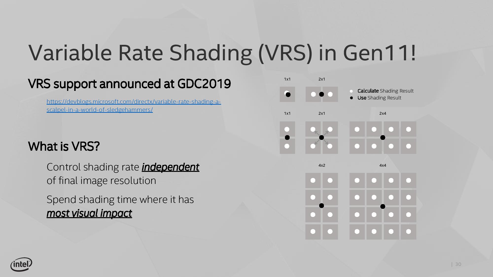
The idea is that using this method can reduce some of the load on the execution units, ultimately increasing the frame rate. The size of that combination of pixels can be adjusted on a per-frame basis as well, allowing the game to take advantage of processing budget where it exists, or pull back to a point where performance is needed. Ultimately Intel believes that any image quality loss is not noticeable, especially for the performance impact they expect it to provide. Intel states that this technology is useful for areas such as lighting adjustments, partially obscured objects (by fog/clouds), and areas that undergo blur, or foveated rendering – basically any area where clarity isn’t explicitly required to begin with.
The only issue here though is an ecosystem one – it requires the game developer support. Intel is already working with Epic to add it to the Unreal Engine, and Intel has worked with developers to enable support in titles such as Civilization 6. The difference in performance, according to Intel, can be up to a 30% FPS increase in a best-case scenario. NVIDIA already supports VRS through dedicated hardware, whereas AMD’s current solutions are best described as a more limited shader-based approximation.


107 Comments
View All Comments
name99 - Wednesday, July 31, 2019 - link
That’s an idiotic chain of reasoning.ARM Macs will ship with macOS, not iOS. To believe otherwise only reveals that you know absolutely nothing of how Apple thinks.
As for comparison, the rough number is A12X gets ~5200 on GB4, Intel best (non-OC’d) gets ~5800. That’s collapsing lots of numbers down to one, but comparing benchmark by benchmark you see Apple does very well (almost matching Intel) across an awful lot.
If Apple can maintain its past pace (and there is no reason why not...) we can expect A13X to be anywhere from 20% to 35% faster, which puts it well into “fastest [non-OC’d] CPU on earth” territory for most single-threaded use cases. Can they achieve this? Absolutely.
Just process improvement can get them 10% frequency. I expect A13X to clock around 2.8GHz.
Then there is LPDDR5 which I expect they will be using, so substantially improved memory bandwidth. Then I expect they'll have SVE (2x256) and accompanying that basically double the bandwidth all the way out from L1 to DRAM.
These are just the obvious basics. There are a bunch of things they can still do that represent “fairly easy” improvements to get to that 25% or so. (These include more aggressive fusion, a double-pumped ALU, attached ALUs to load/store to allow load-ok and op-store fusion, a micro-op cache, long-term-parking, criticality prediction, ...)
So, if it’s so easy, why doesn’t Intel also do it? Why indeed? That’s why I occasionally post my alternative rant about how INTC is no longer an engineering company, it is now pretty much purely a finance company...
ifThenError - Friday, August 2, 2019 - link
Sorry, but both these comments seem mighty uninformed. The MacBooks Air and Pro currently and in the foreseeable future all run on Intel CPUs. The Apple Chips A12/13 are used in iPhone, iPad and the likes.And regarding your prediction, your enthusiasm seems way over the top. What are you even talking about? Micro-op cache on a RISC processor? Think again. Aren't RISC commands all micro ops already?
name99 - Sunday, August 4, 2019 - link
Strong the Dunning-Kruger is with this one...Dude, seriously, learn something about MODERN CPU design, more than just buzz-words from the 80s.
To get you started, how about you read
https://www.anandtech.com/show/14384/arm-announces...
and concentrate on understanding EVERY aspect of what's being added to the CPU and why.
Note in particular that 1.5K Mop cache...
More questions to ask yourself:
- Why was 80s RISC obsessed with REDUCED instructions?
- Why was ARM (especially ARMv8) NOT obsessed with that? Look at the difference between ARMv8 and, say, RISC-V.
- Why is op-fusion so important a part of modern high performance CPUs (both x86 and ARM [and presumably RISC-V if they EVER ship a high-performance part, ha...])?
- which are the fast (shallow logic, even if it's wide) and which are the slow (deep logic) parts of a MODERN pipeline?
ifThenError - Monday, August 5, 2019 - link
Oh my, this is so entertaining you should charge for the reading.You demand to go beyond just buzz words (what would be good) while your posts look like entries to a contest on how many marketing phrases can be fit into a paragraph.
Then you even manage to combine this with highly rude idiom. Plus you name a psychological effect but fail to transfer it to self-reflexion. And as cherry on the top you obviously claim for yourself to understand „EVERY aspect“ of a CPU (an unimaginably complex bit of engineering) but even manage to confuse micro- and macro-op cache and the conceptual differences of these.
I'm really impressed by your courage. Publicly posting so boldly on such a thin basis is brave.
Your comments add near zero information but are definately worth the read. Pure comedy gold!
Please see this as an invitation to reply. I'm looking forwards to some more of your attempts to insult.
Techgeek43 - Tuesday, July 30, 2019 - link
Fantastic article Ian, I for one, cannot wait for ice lake laptopsWonderful in-depth analysis, with an interesting insight into the Intel brand
repoman27 - Tuesday, July 30, 2019 - link
"The high-end design with 64 execution units will be called Iris Plus, but there will be a ‘UHD’ version for mid-range and low-end parts, however Intel has not stated how many execution units these parts will have."Ah, but they have: Ice Lake-U Iris Plus (48EU, 64EU) 15 W, Ice Lake-U UHD (32EU) 15 W. So their performance comparisons may even be to the 15 W Iris Plus with 64 EUs, rather than the full fat 28 W version.
I know you have access to the media slide decks, but Intel has also posted product briefs for the general public that contain a lot of this info: https://www.intel.com/content/www/us/en/products/d...
"On display pipes, Gen11 has access to three 4K pipes split between DP1.4 HBR3 and HDMI 2.0b. There is also support for 2x 5K60 or 1x 4K120 with a 10-bit color depth."
The three display pipes are not limited to 4K, and are agnostic of transport protocol—each of them can be output via the eDP 1.4b port, one of the 3 DDI interfaces which can support either DisplayPort 1.4 or HDMI 2.0b, or one of the up to 4 Thunderbolt 3 ports. Both HDMI and DP support HDCP 2.2, and DisplayPort also supports DSC 1.1. The maximum single pipe, single port resolution for HDMI is 4K60 10bpc (4:2:2), and for DisplayPort it's 4K120/5K60 10bpc (with DSC).
Thunderbolt 3 integration for Ice Lake-Y is only up to 3 ports.
abufrejoval - Tuesday, July 30, 2019 - link
What I personally liked most about the GT3e (48 EU) and GT4e (72 EU) Skylake variant SoCs was, that they didn't cost the extra money they should have, especially when you consider that the iGPU part completely dwarfs the CPU cores (which Intel makes you bleed for) and is much better than everything else combined together (have a look at the WikiChips layoutshttps://en.wikichip.org/wiki/intel/microarchitectu...
Of course, a significantly better graphics performance is never a bad thing, especially when it also doesn't cost extra electrical power: The bigger iGPUs might have actually been more energy efficient than their GT2 brethren at a graphics load that pushed the GT2 towards its frequency limits. And in any case if you don't crunch it on graphics, the idle consumption is near perfect: One of the reasons most laptop dGPU designs won't even bother to run 2D on the dGPU any more but leave that to Intel.
The biggest downside was that you couldn't buy them outside an Apple laptop or Intel NUC.
But however much Intel goes into Apple mode (the major customer for these beefier iGPUs) in terms of "x time faster than previous", the result aren't going to turn ultrabooks with this configuration into "THD gaming machines".
To have a good feel as to where these could go and whether they are worth the wait, just have a look at the Skull Canyon nuc6i7kyk review on this site: That SoC uses 72 EUs and 128MB of eDRAM and should put a pretty firm upper limit to what a 64 EU Ice Lake can do: Most of the games in that review are somewhat dated yet fail to reach 20FPS at THD.
So if you want to game on the device, you'd be much better of with a dGPU however small and chose the smallest iGPU variant available. No reason to wait, Whisky + Nvidia will do better.
If you want real gaming performance, you need to put real triple digit Watts and the bandwidth only GDDR5/6 or HBM can deliver to work even at THD, but with remote gaming perhaps it doesn't have to be on your elegant slim ultrabook. There again anything but the GT2 configuration is wasted, because only need the VPU part for decoding Google Stadia (or Steam Remote) streams, which is the same for all configurations.
For some strange reason, Intel has been selling GT3/4 NUCs at little or no premium over GT2 variants and in that case I have been seriously tempted. And only once I even managed to find a GT3e laptop once for a GT2 price (while the SoC is literally twice as big and the die carrier even adds eDRAM at zero markup), which I stil cherish.
But if prices are anywhere related to the surface area of the chip (as they are for the server parts), these high powered GTs are something that only Apple users would buy.
That's another reaons, I (sadly) don't expect them to be sold in anything bug Macs and some NUCs, no ChuWi notebooks or Mini-ITX boards.
abufrejoval - Tuesday, July 30, 2019 - link
...(need edit)Judging from the first 10nm generation, GPUs where the part where obtaining economically feasible yields didn't work out. Unless they have really, really fixed 10nm it's not hard to imagine that Intel could be selling high-count EU SoCs to Apple below cost, to keep them for another generation as flagship customer and perhaps due to long-term contractual obligations.
But maintaining GT2/3/4 price egality for the rest of the market seems suicidal even if you have a fab lead.
Not that I expect we'll ever be told: In near monopoly situations the so called market ecnomy becomes surprisingly complex.
willis936 - Wednesday, July 31, 2019 - link
What the hell is a THD in this context?jospoortvliet - Monday, August 5, 2019 - link
Probably full HD (True HD)?