Examining Intel's Ice Lake Processors: Taking a Bite of the Sunny Cove Microarchitecture
by Dr. Ian Cutress on July 30, 2019 9:30 AM EST- Posted in
- CPUs
- Intel
- 10nm
- Microarchitecture
- Ice Lake
- Project Athena
- Sunny Cove
- Gen11
Sunny Cove Microarchitecture: Going Deeper and Wider
Ice Lake falls under Intel’s ‘10th Gen Core’ family, and is based around the latest iteration of the ‘Core’ microarchitecture, which initially debuted over a decade ago and has received plenty of key critical enhancements and extra features along the way. Over the years we’ve seen improved prefetchers, smarter branch predictors, adjusted cache sizes and capabilities, deeper and wider execution, micro-op caches, accelerated calculation logic, and lower power operation, all designed to increase the instruction throughput, decrease cache misses, and improve power efficiency.
When Intel designs a new generation of Core, it tends to go in a lot of things: mobile CPUs, desktops, servers, sometimes embedded, new communications technologies, and plenty of other custom silicon besides. As a result, it has to scale, from low-end to high-end. One of Intel’s new Chief Architects, Jim Keller, says that Intel has a ‘milliwatt-to-megawatt’ strategy when it comes to product design, and it’s the Core microarchitecture that is currently bringing in the big $$$ to fund a lot of the R&D.
Before we go into the new Sunny Cove core, I should preface the explanations with a little warning. Intel’s previous microarchitecture update and design, Skylake, is Intel’s most profitable design ever. Part of that reason is that it has been around the block for four generations of products. Intel hasn’t changed the core in that time, for almost four years. At this point, we’ve been yearning for something that actually has changes. So please forgive a little excitement when covering a few of the more mundane updates.
Sunny Cove Front End
Despite the instruction entry point into the core being at the front-end. Intel didn’t say too much about Sunny Cove in this respect. Typically Intel keeps the details of its prefetchers and branch predictors secret, although CPU Architect Ronak Singhal did state that it is by-and-large similar to the Skylake design. Ronak has said that the branch predictor has increased accuracy, and that the average/effective load latency has decreased, and by and large the front-end of the CPU has been optimized for client (read consumers/end-users), rather than servers, which Skylake was. The internal structures of the branch predictor unit and prefetcher are larger according to Intel, which should help improve accuracy.
The L1 instruction cache is still a 32 KiB 8-way design, and there are still five decoders in play. These decoders are split as one complex decoder and four simple decoders, and they can supply up to five micro-ops per cycle. There’s nothing drastically new in terms of op fusion we are told, just the general expected improvements, plus additional support for the new AVX-512 instructions.
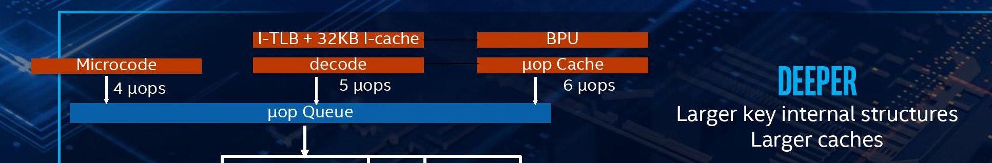
The micro-op cache gets an update here, from 1.5k entries to 2.25k entries. This is the first time that Intel has increased the micro-op cache size since Haswell, but it should be noted that the competition also has micro-op caches (ARM has 1.5k, AMD has 2k for Zen, 4k for Zen 2), and so refinement in this area is going to be critical. The micro-op cache can supply six micro-ops to the queue per cycle.
Overall, six micro-ops can be fed between the decoders/cache/direct micro-code per cycle. That is split between up to six per cycle from the cache, up to 5 from the decoders, and up to 4 from direct microcode (which gets fed through the complex decoder.
Out-of-Order Window
The micro-op queue, for rename/allocate/retire, has also increased. The design went from 182 micro-ops in Haswell to 224 in Skylake, but goes all the way up to 352 in Sunny Cove, a massive 57% increase. This will help managing which instructions are ready to be processed by the scheduler, although this often comes at the penalty of power. This is one of the advantages of using a smaller process node – there’s more power budget to go around, allowing a CPU team to design bigger queues.
| AnandTech | Haswell | Skylake | Sunny Cove |
| Reorder Buffer | 182 | 224 | 352 |
| In-Flight Stores | 72 | 72 | 128 |
| In-Flight Loads | 42 | 56 | 72 |
With the increased queue size, Intel also reports that support for in-flight loads and stores has increased: up from 72 loads in Skylake to 128 in Sunny Cove, and up from 56 stores in Skylake to 72 in Sunny Cove. This means that the in-flight load/store ratio is more weighted in favor of loads, which Intel states is part of the more user-focused design where loads end up being more important than stores.
Back End
This is where the fun happens. As with previous Intel designs over the years, we still have a unified scheduler for both integer and vector operations, however they are split between four different reservation stations depending on what operation is needed:
- One for four ALU ports, accepts 4 micro-ops/cycle
- One for two Store ports, accepts 2 micro-ops/cycle
- One for a pair of AGUs, one load, one store, accepts 2 micro-ops/cycle
- One for a pair of AGUs, one load, one store, accepts 2 micro-ops/cycle
In total, the number of execution ports has increased from 8 in Skylake to 10 in Sunny Cove. This allows for 10 micro-ops per cycle to be dispatched from the reorder buffer, a 25% increase. The two new ports lie in different areas: Skylake had 3 AGUs, supporting two loads and one store per cycle, but Sunny Cove now has 4 AGUs, for two loads and two stores per cycle. The other new port is a store data port. With these changes, the L1 data cache can now support two stores per cycle, effectively doubling the L1 store bandwidth.
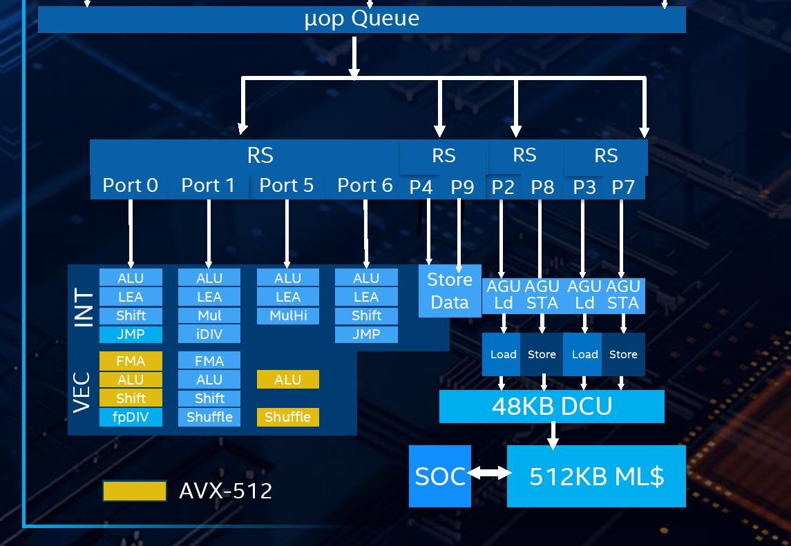
The L1 Data cache has increased, for the first time in over a decade. Intel has moved from a 32 KiB 8-way design up to a 48 KiB 12-way design, which should help reduce data cache misses significantly. This combined with the micro-op cache size increase is one of the easiest ways to reduce cache miss penalties. (For comparison, in Zen 2 AMD halved its L1-I size and doubled its micro-op cache, which it felt was a more efficient way of improving instruction throughput, but also the silicon area design had to be managed.)
Intel has also increased the L2 cache, up from 256 KiB to 512 KiB, and it is still non-inclusive of the L1 with a write-back policy. In order to assist the L2, the L2 TLB page table arrangement has also been improved, with up to 2k entries at 4K, 1k entries for 2M/4M (new, used to be shared with 4K), and up from 16 entries to 1024 entries at 1G. The cache improvements on Sunny Cove are certainly expected to work in Intel’s favor, especially when it comes to the enhanced graphics part of the design.
On a core-to-core level, Intel's recent designs have the following configurations:
| Microarchitecture Comparison | ||||||
| Skylake | Cannon Lake | Sunny Cove* | Zen | Zen 2 | ||
| L1-D Cache |
32 KiB/core 8-way |
32 KiB/core 8-way |
48 KiB/core 12-way |
32 KiB/core 8-way |
32 KiB/core 8-way |
|
| L1-I Cache |
32 KiB/core 8-way |
32 KiB/core 8-way |
32 KiB/core 8-way |
64 KiB/core 4-way |
32 KiB/core 8-way |
|
| L2 Cache |
256 KiB/core 4-way |
256 KiB/core 4-way |
512 KiB/core 8-way |
512 KiB/core 8-way |
512 KiB/core 8-way |
|
| L3 Cache |
2 MiB/core 16-way |
2 MiB/core 16-way |
2 MiB/core 16-way |
2 MiB/core | 4 MiB/core | |
| L3 Cache Type | Inclusive | Inclusive | Inclusive | Non-Inclusive | Non-Inclusive | |
| Decode | 4 + 1 | 4 + 1 | 4 + 1 | 4 | 4 | |
| uOP Cache | 1.5k | 1.5k | 2.25k | 2k | 4k | |
| Reorder Buffer | 224 | 224 | 352 | 192 | 224 | |
| Execution Ports | 8 | 8 | 10 | 10 | 11 | |
| AGUs | 2 + 1 | 2 + 1 | 2 + 2 | 1 + 1 | 2 + 1 | |
| AVX-512 | - | 1 x FMA | 1 x FMA | - | ||
| * Sunny Cove numbers for Client. Server will have different L2/L3 cache and FMA, like Skylake | ||||||
For the execution ports, now that Intel has moved AVX-512 into the mainstream Core design, there are a few changes. AVX-512 is now supported on Port 0 (FMA, ALU, Shift) and Port 5 (ALU, Shuffle). There is only one AVX-512 port, but also a 256-bit FMA port, so either 1x512-bit or 2x256-bit throughput is possible.
Overall the design allows for:
| Back-End Execution Resources | ||||||||
| Skylake | Port | Sunny Cove | ||||||
| Integer | ||||||||
| JMP | Shift | ALU | 0 | ALU | LEA | Shift | JMP | |
| LEA | ALU | 1 | ALU | LEA | Mul | iDIV | ||
| Mul | LEA | ALU | 5 | ALU | LEA | MulHi | ||
| JMP | Shift | ALU | 6 | ALU | LEA | Shift | JMP | |
| Vector / FP | ||||||||
| fpDIV | Shift | ALU | FMA | 0 | FMA | ALU | Shift | fpDIV |
| Shift | ALU | FMA | 1 | FMA | ALU | Shift | Shuffle | |
| Shuffle | ALU | FMA | 5 | FMA | ALU | Shuffle | ||
The parts highlighted in bold are different in the Sunny Cove core.
The TL;DR
The core improvements can be summed up as follows:
- Better prefetchers and branch predictors
- +50% L1 Data Cache
- +100% L1 Store Bandwidth
- +100% L2 Cache w/improved L2 TLB
- +50% Micro-op Cache
- +25% uops/cycle into reorder buffer
- +57% reorder buffer size
- +25% execution ports
- AVX-512 with VNNI
Add in better memory support (Up to LPDDR4X-3733) and better graphics (64 EUs of Gen11), and it’s a really nice update.
For all of this, Intel is promoting a +18% IPC increase over Skylake, which ranges from 0.98x to 1.40x depending on the workload (SPEC2006, SPEC2017, SYSMark 2014SE, WebXPRT, CineBench), or a +47% increase in real world tasks against Broadwell.

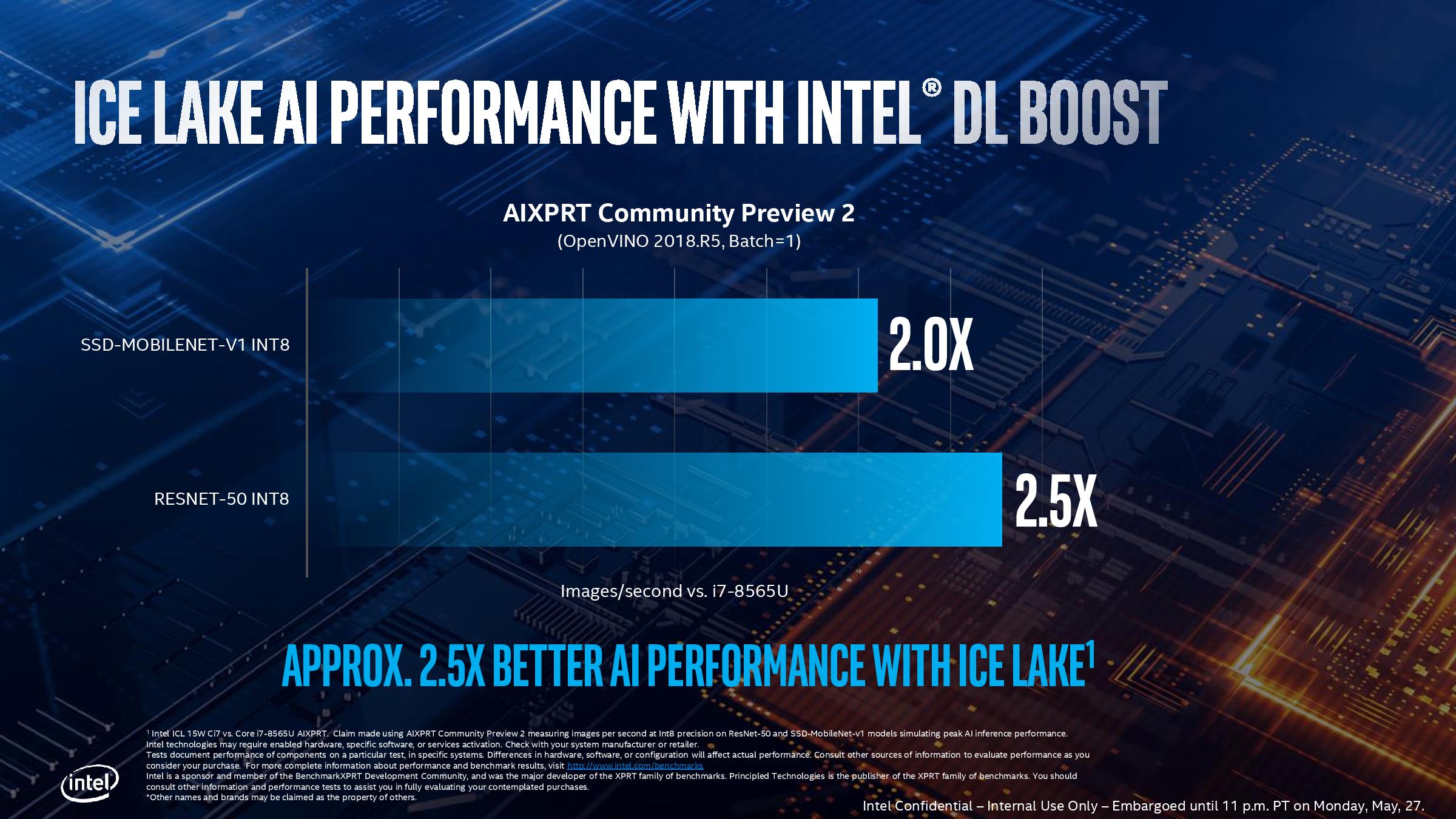
When AVX512 is in play, with DLBoost, Intel is promoting a 2.0x-2.5x increase against the best Whiskey Lake has to offer.
We’ll cover Intel’s claims later in the analysis.


107 Comments
View All Comments
name99 - Wednesday, July 31, 2019 - link
That’s an idiotic chain of reasoning.ARM Macs will ship with macOS, not iOS. To believe otherwise only reveals that you know absolutely nothing of how Apple thinks.
As for comparison, the rough number is A12X gets ~5200 on GB4, Intel best (non-OC’d) gets ~5800. That’s collapsing lots of numbers down to one, but comparing benchmark by benchmark you see Apple does very well (almost matching Intel) across an awful lot.
If Apple can maintain its past pace (and there is no reason why not...) we can expect A13X to be anywhere from 20% to 35% faster, which puts it well into “fastest [non-OC’d] CPU on earth” territory for most single-threaded use cases. Can they achieve this? Absolutely.
Just process improvement can get them 10% frequency. I expect A13X to clock around 2.8GHz.
Then there is LPDDR5 which I expect they will be using, so substantially improved memory bandwidth. Then I expect they'll have SVE (2x256) and accompanying that basically double the bandwidth all the way out from L1 to DRAM.
These are just the obvious basics. There are a bunch of things they can still do that represent “fairly easy” improvements to get to that 25% or so. (These include more aggressive fusion, a double-pumped ALU, attached ALUs to load/store to allow load-ok and op-store fusion, a micro-op cache, long-term-parking, criticality prediction, ...)
So, if it’s so easy, why doesn’t Intel also do it? Why indeed? That’s why I occasionally post my alternative rant about how INTC is no longer an engineering company, it is now pretty much purely a finance company...
ifThenError - Friday, August 2, 2019 - link
Sorry, but both these comments seem mighty uninformed. The MacBooks Air and Pro currently and in the foreseeable future all run on Intel CPUs. The Apple Chips A12/13 are used in iPhone, iPad and the likes.And regarding your prediction, your enthusiasm seems way over the top. What are you even talking about? Micro-op cache on a RISC processor? Think again. Aren't RISC commands all micro ops already?
name99 - Sunday, August 4, 2019 - link
Strong the Dunning-Kruger is with this one...Dude, seriously, learn something about MODERN CPU design, more than just buzz-words from the 80s.
To get you started, how about you read
https://www.anandtech.com/show/14384/arm-announces...
and concentrate on understanding EVERY aspect of what's being added to the CPU and why.
Note in particular that 1.5K Mop cache...
More questions to ask yourself:
- Why was 80s RISC obsessed with REDUCED instructions?
- Why was ARM (especially ARMv8) NOT obsessed with that? Look at the difference between ARMv8 and, say, RISC-V.
- Why is op-fusion so important a part of modern high performance CPUs (both x86 and ARM [and presumably RISC-V if they EVER ship a high-performance part, ha...])?
- which are the fast (shallow logic, even if it's wide) and which are the slow (deep logic) parts of a MODERN pipeline?
ifThenError - Monday, August 5, 2019 - link
Oh my, this is so entertaining you should charge for the reading.You demand to go beyond just buzz words (what would be good) while your posts look like entries to a contest on how many marketing phrases can be fit into a paragraph.
Then you even manage to combine this with highly rude idiom. Plus you name a psychological effect but fail to transfer it to self-reflexion. And as cherry on the top you obviously claim for yourself to understand „EVERY aspect“ of a CPU (an unimaginably complex bit of engineering) but even manage to confuse micro- and macro-op cache and the conceptual differences of these.
I'm really impressed by your courage. Publicly posting so boldly on such a thin basis is brave.
Your comments add near zero information but are definately worth the read. Pure comedy gold!
Please see this as an invitation to reply. I'm looking forwards to some more of your attempts to insult.
Techgeek43 - Tuesday, July 30, 2019 - link
Fantastic article Ian, I for one, cannot wait for ice lake laptopsWonderful in-depth analysis, with an interesting insight into the Intel brand
repoman27 - Tuesday, July 30, 2019 - link
"The high-end design with 64 execution units will be called Iris Plus, but there will be a ‘UHD’ version for mid-range and low-end parts, however Intel has not stated how many execution units these parts will have."Ah, but they have: Ice Lake-U Iris Plus (48EU, 64EU) 15 W, Ice Lake-U UHD (32EU) 15 W. So their performance comparisons may even be to the 15 W Iris Plus with 64 EUs, rather than the full fat 28 W version.
I know you have access to the media slide decks, but Intel has also posted product briefs for the general public that contain a lot of this info: https://www.intel.com/content/www/us/en/products/d...
"On display pipes, Gen11 has access to three 4K pipes split between DP1.4 HBR3 and HDMI 2.0b. There is also support for 2x 5K60 or 1x 4K120 with a 10-bit color depth."
The three display pipes are not limited to 4K, and are agnostic of transport protocol—each of them can be output via the eDP 1.4b port, one of the 3 DDI interfaces which can support either DisplayPort 1.4 or HDMI 2.0b, or one of the up to 4 Thunderbolt 3 ports. Both HDMI and DP support HDCP 2.2, and DisplayPort also supports DSC 1.1. The maximum single pipe, single port resolution for HDMI is 4K60 10bpc (4:2:2), and for DisplayPort it's 4K120/5K60 10bpc (with DSC).
Thunderbolt 3 integration for Ice Lake-Y is only up to 3 ports.
abufrejoval - Tuesday, July 30, 2019 - link
What I personally liked most about the GT3e (48 EU) and GT4e (72 EU) Skylake variant SoCs was, that they didn't cost the extra money they should have, especially when you consider that the iGPU part completely dwarfs the CPU cores (which Intel makes you bleed for) and is much better than everything else combined together (have a look at the WikiChips layoutshttps://en.wikichip.org/wiki/intel/microarchitectu...
Of course, a significantly better graphics performance is never a bad thing, especially when it also doesn't cost extra electrical power: The bigger iGPUs might have actually been more energy efficient than their GT2 brethren at a graphics load that pushed the GT2 towards its frequency limits. And in any case if you don't crunch it on graphics, the idle consumption is near perfect: One of the reasons most laptop dGPU designs won't even bother to run 2D on the dGPU any more but leave that to Intel.
The biggest downside was that you couldn't buy them outside an Apple laptop or Intel NUC.
But however much Intel goes into Apple mode (the major customer for these beefier iGPUs) in terms of "x time faster than previous", the result aren't going to turn ultrabooks with this configuration into "THD gaming machines".
To have a good feel as to where these could go and whether they are worth the wait, just have a look at the Skull Canyon nuc6i7kyk review on this site: That SoC uses 72 EUs and 128MB of eDRAM and should put a pretty firm upper limit to what a 64 EU Ice Lake can do: Most of the games in that review are somewhat dated yet fail to reach 20FPS at THD.
So if you want to game on the device, you'd be much better of with a dGPU however small and chose the smallest iGPU variant available. No reason to wait, Whisky + Nvidia will do better.
If you want real gaming performance, you need to put real triple digit Watts and the bandwidth only GDDR5/6 or HBM can deliver to work even at THD, but with remote gaming perhaps it doesn't have to be on your elegant slim ultrabook. There again anything but the GT2 configuration is wasted, because only need the VPU part for decoding Google Stadia (or Steam Remote) streams, which is the same for all configurations.
For some strange reason, Intel has been selling GT3/4 NUCs at little or no premium over GT2 variants and in that case I have been seriously tempted. And only once I even managed to find a GT3e laptop once for a GT2 price (while the SoC is literally twice as big and the die carrier even adds eDRAM at zero markup), which I stil cherish.
But if prices are anywhere related to the surface area of the chip (as they are for the server parts), these high powered GTs are something that only Apple users would buy.
That's another reaons, I (sadly) don't expect them to be sold in anything bug Macs and some NUCs, no ChuWi notebooks or Mini-ITX boards.
abufrejoval - Tuesday, July 30, 2019 - link
...(need edit)Judging from the first 10nm generation, GPUs where the part where obtaining economically feasible yields didn't work out. Unless they have really, really fixed 10nm it's not hard to imagine that Intel could be selling high-count EU SoCs to Apple below cost, to keep them for another generation as flagship customer and perhaps due to long-term contractual obligations.
But maintaining GT2/3/4 price egality for the rest of the market seems suicidal even if you have a fab lead.
Not that I expect we'll ever be told: In near monopoly situations the so called market ecnomy becomes surprisingly complex.
willis936 - Wednesday, July 31, 2019 - link
What the hell is a THD in this context?jospoortvliet - Monday, August 5, 2019 - link
Probably full HD (True HD)?