Intel's 10nm Cannon Lake and Core i3-8121U Deep Dive Review
by Ian Cutress on January 25, 2019 10:30 AM ESTUncovering the Microarchitecture Secrets
When we approached Intel to see if they would disclose the full microarchitecture, just as usually do in the programming manuals for all the other microarchitectures they’ve released, the response was underwhelming. There is one technical document related to Cannon Lake I can’t access without a corporate NDA, which would be no use for an article like this. These documents usually fall under corporate NDA before the official launch, and eventually become public a short time after. However, when we requested the document, as well as details on the microarchitecture, we received a combination of ‘we’re not disclosing it at this time’ and ‘well tell us what you’ve found and we’ll tell you what is right’. That was less helpful than I anticipated.
As a result I pulled in a few helpful peers around the industry to try and crack this egg. Here’s what we think Cannon Lake looks like.
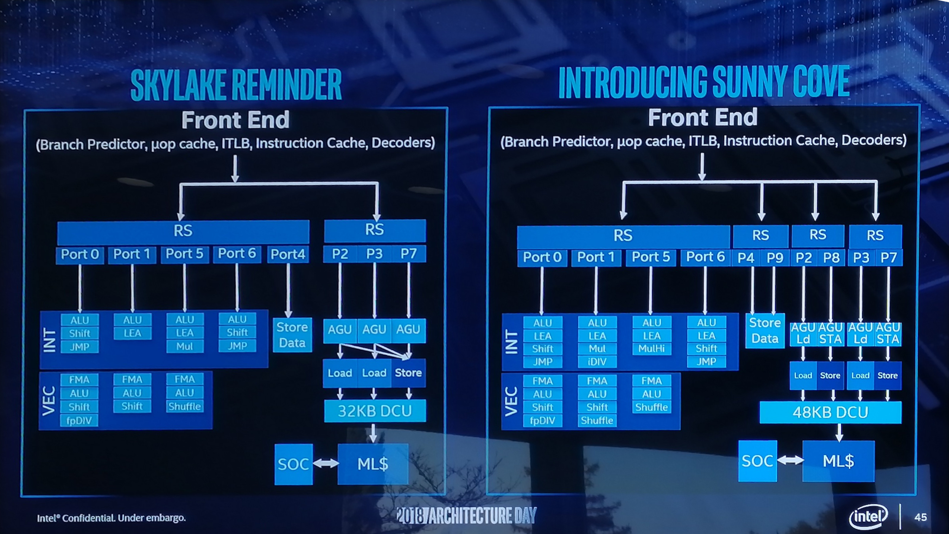
On the whole, the system is ultimately designed as a mix between the Skylake Desktop core and the Skylake-SP core from the enterprise world. While it has a standard Skylake design using a 4+1 decode and eight execution ports, along with a standard Skylake desktop L1+L2+L3 cache structure, it brings over a single AVX-512 port from the enterprise side as well as support for 2x512B/cycle read from the L1D cache and 1x512B/cycle write.
What we’ve ended up here is with a hybrid of the Skylake designs. To go even further, it’s also part of the way to a Sunny Cove core, Intel’s future second generation 10nm core design which the company disclosed part of in December. This is based on some of the instruction features not present in Skylake but found on both Cannon Lake and Sunny Cove.
Mostly Column A, A Little of Column B
It’s mostly desktop Skylake at the end of the day – both Cannon Lake and Sunny Cove have the same AVX512 compatibility, just with the Skylake cache structure. We’re not too clear on most front end changes on Cannon Lake as those are difficult to measure, although we can tell that the re-order buffer size is the same as Skylake (224 uops). However, most of the features mentioned in the Sunny Cove announcement (doubling store bandwith, more execution ports, and capabilities per execution port) are not in Cannon Lake.
| Microarchitecture Comparison | ||||||
| Skylake Desktop |
Skylake Xeon |
Cannon Lake | Sunny Cove* | Ryzen | ||
| L1-D Cache |
32 KiB/core 8-way |
32 KiB/core 8-way |
32 KiB/core 8-way |
48 KiB/core ?-way |
64 KiB/core 4-way |
|
| L1-I Cache |
32 KiB/core 8-way |
32 KiB/core 8-way |
32 KiB/core 8-way |
? | 32 KiB/core 8-way |
|
| L2 Cache |
256 KiB/core 4-way |
1 MiB/core 16-way |
256 KiB/core 4-way |
256 KiB/core ?-way |
512 KiB/core 8-way |
|
| L3 Cache |
2 MiB/core 16-way |
1.375 MiB/core 11-way |
2 MiB/core 16-way |
? | 2 MiB/core | |
| L3 Cache Type | Inclusive | Non-Inclusive | Inclusive | ? | Non-Inclusive | |
| Decode | 4 + 1 | 4 + 1 | 4 + 1 | 5(?) + 1 | 4 | |
| uOP Cache | 1536 | 1536 | 1536 (?) | >1536 | ~2048 | |
| Reorder Buffer | 224 | 224 | 224 | ? | 192 | |
| Execution Ports | 8 | 8 | 8 | 10 | 10 | |
| AGUs | 2 + 1 | 2 + 1 | 2 + 1 | 2 + 2 | 2 | |
| AVX-512 | - | 2 x FMA | 1 x FMA | ? x FMA | - | |
| * Sunny Cove numbers for Client. Server will have different L2/L3 cache and FMA, like Skylake | ||||||
There are several parts to the story on Cannon Lake:
- New Instructions and AVX-512 Instruction Support
- Major Changes in Existing Instructions and Other Minor Changes
New Instructions and AVX-512 Instruction Support
The three new instructions supported on Cannon Lake are Integer Fused Multiply Add (IFMA), Vector Byte Manipulation Instructions (VBMI), and hardware based SHA (Secure Hash Algorithm) support. Intel has already stated that IFMA is supported on Ice Lake/Sunny Cove, although no word on VBMI. The hardware based SHA is already present in Goldmont, however our tests show the Goldmont version is actually better.
IFMA is a 52-bit Integer fused multiply add (FMA) behaves identically to AVX512 floating point FMA, offering a latency of four clocks and a throughput of two per clock (for xmm/ymm, zmm is four and one). This instruction is commonly listed as helping cryptographic functionality, but also means there is now added support for arbitrary precision arithmetic. Alexander Yee, the developer of the hyper optimized mathematical constant calculator y-cruncher, explained to be why IFMA helps his code when calculating constants like Pi:
The standard double-precision floating-point hardware in Intel CPUs has a very powerful multiplier that has been there since antiquity. But it couldn't be effectively tapped into because that multiplier was buried inside the floating-point unit. The SIMD integer multiply instructions only let you utilize up to 32x32 out of the 52x52 size of the double-precision multiply hardware with additional overhead needed. This inefficiency didn't go unnoticed, so people ranted about it, hence why we now have IFMA.
The main focus of research papers on this is that big number arithmetic that wants the largest integer multiplier possible. On x64 the largest multiplier was the 64 x 64 -> 128-bit scalar multiply instruction. This gives you (64*64 = 4096 bits) of work per cycle. With AVX512, the best you can do is eight 32 x 32 -> 64-bit multiply via the VPMULDQ instruction, which gets you (8 SIMD lanes * 32*32 * 2FMA = 16384 bits) of work per cycle. But in practice, it ends up being about half of that because you have the overhead of additions, shifts, and shuffles competing for the same execution ports.
With AVX512-IFMA, users can unleash the full power of the double-precision hardware. A low/high IFMA pair will get you (8 SIMD lanes * 52*52 = 21632 bits) of work. That's 21632/cycle with 2 FMAs or 10816/cycle with 1 FMA. But the fused addition and 12 "spare bits" allows the user to eliminate nearly all the overhead that is needed for the AVX512-only approach. Thus it is possible to achieve nearly the full 21632/cycle of efficiency with the right port configuration (CNL only has 1 FMA).
There's more to the IFMA arbitrary precision arithmetic than just the largest multiplier possible. RSA encryption is probably one of the only applications that will get the full benefit of the IFMA as described above. y-cruncher benefits partially. Prime95 will not benefit at all.
For the algorithms that can take advantage of it, this boils down to the following table:
| IFMA Performance | |||
| Scalar x64 | AVX512-F | AVX512-IFMA | |
| Single 512b FMA | 4096-bit/cycle | ~4000-bit/cycle | 10816-bit/cycle |
| Dual 512b FMA | 4096-bit/cycle | ~8000-bit/cycle | 21632-bit/cycle |
VBMI is useful in byte shuffling scenarios, offering several instructions:
| VBMI Intructions | |||
| Description | Latency | Throughput | |
| VPERMB | 64-byte any-to-any shuffle | 3 clocks | 1 per clock |
| VPERMI2B | 128-byte any-to-any overwriting indexes |
5 clocks | 1 per 2 clocks |
| VPERMT2B | 128-byte any-to-any overwriting tables |
5 clocks | 1 per 2 clocks |
| VPMULTISHIFTQB | Base64 conversion | 3 clocks | 1 per clock |
Alex says that y-cruncher could benefit from VBMI, however it is one of those things he has to test with hardware on hand rather than on an emulator. Intel hasn’t specified if the Sunny Cove core supports VBMI, which would be an interesting omission.
For hardware accelerated SHA, this is designed purely to accelerate cryptography. However our tools show that the Cannon Lake implementation is slower than both Ryzen and Goldmont, which means it isn’t particularly useful. Cannon Lake also supports Vector-AES, which allows AES instructions to use more of the AVX-512 unit at once, multiplying throughput. Intel has stated that Sunny Cove has implemented SHA and SHA-NI instructions, along with Galois Field instructions and Vector-AES, although to what extent we do not know.
Changes in Existing Instructions
Most generations, Intel will add additional logic to improve the instructions already in place, typically for increasing throughput or decreasing latency (or both).
The big change here is with 64-bit integer divisions now being hardware supported, rather than split into several instructions. Divisions are time consuming at the best of times, however implementing a hardware radix divider means that Cannon Lake can complete at 64-bit IDIV in 18 clocks, compared to 45 on Ryzen and 97 on Skylake. This adjustment is also in the second generation 10nm Sunny Cove core.
For block storage of strings, all of the REP STOS* series of instructions can now use the 512-bit execution write port, allowing a throughput of 61 bits per clock, compared to 43 on Skylake-SP, 31 on Skylake, and 14 on Ryzen.
The AVX512BW command VPERMW, for permuting word integer vectors, has decreased in latency from six clocks to four clocks, and doubled throughput to one per clock compared to one per two clocks. Similarly with vectors, moving or merging vectors of single or double precision scalars using VMOVSS and VMOVSD commands now behaves identically to other MOV commands. This is also present in Sunny Cove.
Other beneficial adjustments to the instruction set include making ZMM divisions and square roots one clock faster, and increasing throughput of some GATHER functions from one per four clocks to one per three clocks.
Regressions come in the form of old x87 commands, with x87 DIV, SQRT, REP CMPS, LFENCE, and MFENCE all being one clock slower. Other x87 transcendentals are many clocks slower, with the goal of deprecation.
There other points to mention:
The VPCONFLICT* commands, which had a latency of 3 clocks and a throughput of one per clock are still slow on Cannon Lake, with the DWORD ZMM form having a latency of 26 clocks and a throughput of one per 20 clocks. This change has not made its way across platforms as of yet.
The cache line write back function, CLWB, was introduced in Skylake-SP to help assist with persistent memory support. It writes back modified data of a cache line, but avoids invalidating the line from the cache (and instead transitions the line to non-modified state). CLWB attempts to minimize the compulsory cache miss if the same data is accessed temporally after the line is flushed if the same data is accessed temporally after the line is flushed. The idea is that this instruction will help with Optane Persistent DC Memory and databases, hence its inclusion in SKL-SP, however it is not in Cannon Lake. Intel’s own documents suggest it will be a feature in Sunny Cove.
There is also no Software Guard Extension (SGX) support on Cannon Lake.


129 Comments
View All Comments
dgingeri - Saturday, January 26, 2019 - link
With Intel recently releasing the "F" SKUs for processors that don't have integrated graphics, I would think this processor would be a Core i3-8121FU.KOneJ - Sunday, January 27, 2019 - link
ROFL, mate. Though a UF line-up honestly wouldn't surprise me with where MCMs, TSVs, yields, iGPUs, and core counts are seemingly headed.Piotrek54321 - Saturday, January 26, 2019 - link
I would love an article on how quantum mechanical effects have to be taken into account at such small nodes.KOneJ - Sunday, January 27, 2019 - link
I would love to see the mathematics of quantum mechanics cleaned up to be more elegant and less Newtonian in nature.Rudde - Saturday, January 26, 2019 - link
I looked into the transistor density of different nodes and particularily the claim that Intel 10nm will feature "100 million transistors per square millimeter."Intel seems to historically lack in transistor density. 22nm has ~8 million per mm², while competing 28nm from GlobalFoundries have ~13 and TSMC has ~12.
Moving unto 14nm and all foundries double their transistor density. Intel goes to 15M/mm², GF to 24 (on a node bought from Samsung) and TSMC's 16nm also to 24M/mm².
TSMC's 7nm node has a density of ~40M/mm².
Now Intel has made two statements (both found in the first page of the article):
1. 100 million transistors per mm² or a 5.7x improvement.
2. A 2.7x improvement in density over 14nm, which gives 55M/mm². 55M/mm² would be consistent with Intel's claim of beating TSMC's 7nm.
Next I'm assuming my calculations about Intel's transistor density are wrong, and that both of Intels claims are true. In that case Intel's current 14nm would be 27M/mm². Now of course we can't assume my calculations about GF and TSMC are correct either and we are left without any conclusion.
Rudde - Saturday, January 26, 2019 - link
I jumped the gun too early and didn't proceed to page two that explains a lot of the same things as I tries to explain, but uses actual node data and not chip sizes.smalM - Saturday, January 26, 2019 - link
Page two doesn't use actual node data, it uses Intel propaganda ;-)KOneJ - Sunday, January 27, 2019 - link
Yep, they're not the only ones optimizing libraries. They're trying to muddle transistors with design compiling. While this is fair, it's not taking into account that others are working both halves of the problem as well. Clearly meant to be misleading.sidm2k11 - Saturday, January 26, 2019 - link
How is the fan noise on the PN60? Mine makes a pretty loud whine all the time and temperatures regularly cross 80 on full load...My 4010u Brix PC is whisper quiet by comparison.alacard - Saturday, January 26, 2019 - link
Well that was a wonderfully intricate review. Thank you.