Intel's 10nm Cannon Lake and Core i3-8121U Deep Dive Review
by Ian Cutress on January 25, 2019 10:30 AM ESTIntel’s 10nm Cannon Lake Silicon Design
Many thanks to David Schor of WikiChip for his articles on Intel’s 10nm. This page uses his material extensively as the primary source. I highly recommended several of his articles, including his write-ups from IEDM 2017, ISSCC 2018, IEDM 2018, and his page on Cannon Lake.
Measuring The Chip
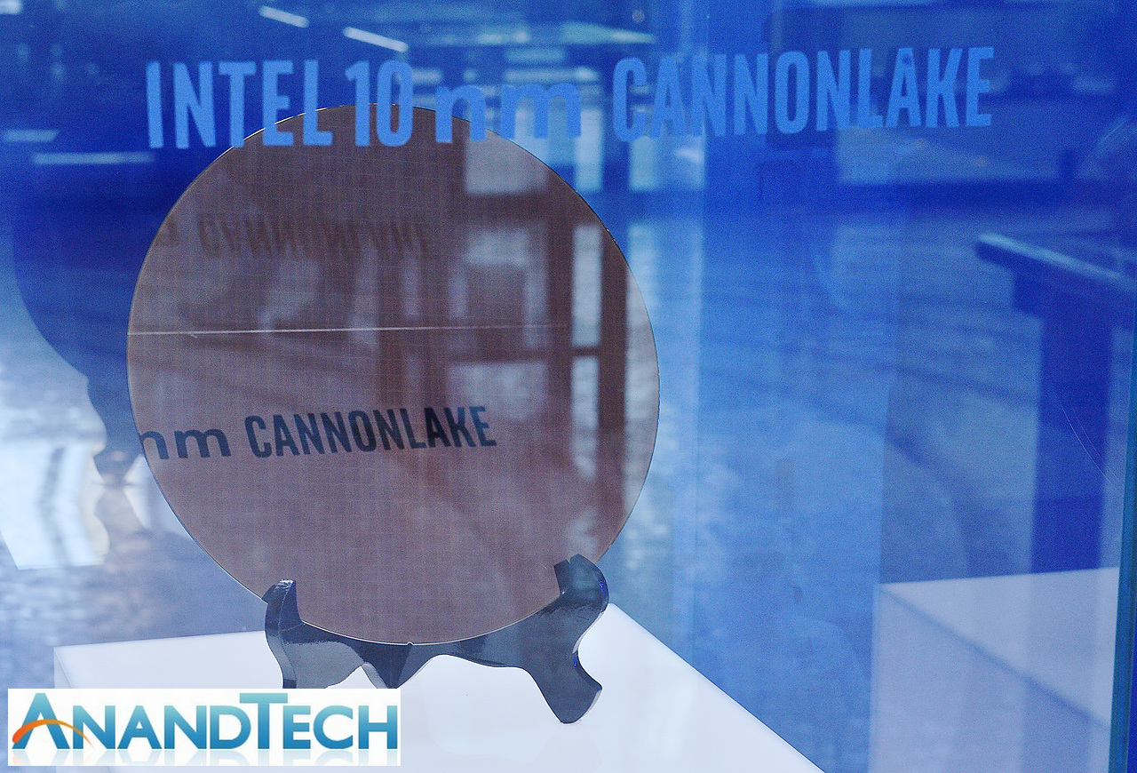
The first true glimpse of a physical Cannon Lake chip, beyond the brief showing of what was supposedly an early Cannon Lake laptop at CES 2017, was during the Chinese version of Intel’s Technology and Manufacturing day in September 2017. Intel presented a full 300mm wafer of Cannon Lake 10nm chips, and through luck we were able to get some clear definition of the chips.
Based on this wafer, we estimated that the chip would be around 70.5 mm2 of die area, and at the time we assumed this was a dual core design with ‘GT2’ graphics, the standard graphics configuration. After the Lenovo Ideapad was made available in China, the experts at TechInsights got hold of a unit and took their saws to the design.
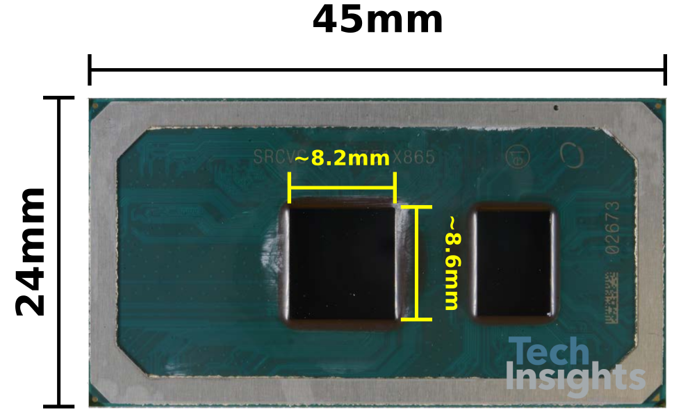
Photo: Techinsights, Measurements by WikiChip
It turns out we weren’t too far off on the die area. This photo of the chip in the system (with IO die on the right) gives a die area of 70.52 mm2, well within an acceptable margin of error. This chip does indeed have two Cannon Lake CPU cores, and 40 Gen10 execution units on the integrated graphics, although the graphics are disabled. This qualifies as a 2+2 design.
For comparison to Intel’s previous dual core designs, this marks Intel’s smallest dual-core design to date. The nearest would be Broadwell, at 82 mm2, but this chip also had a lower proportion of integrated graphics compared to Skylake and newer.
The Ultimate Metric: Transistors Per mm2
One of the metrics used for determining how good a semiconductor process is relates to how many transistors per square millimeter are in a standard chip made on that process. A processor isn’t all transistors though – there are SRAM cells, and also ‘dead’ silicon designed to act as thermal buffers between areas in order to increase the longevity of the parts. There are also different ways to count transistors, as a 2-input NAND logic cell is much smaller than a complex scan flip-flop logic cell, for example. Nonetheless, most in the industry have this metric as a key factor when discussing processes, and hitting certain milestones is usually congratulatory.
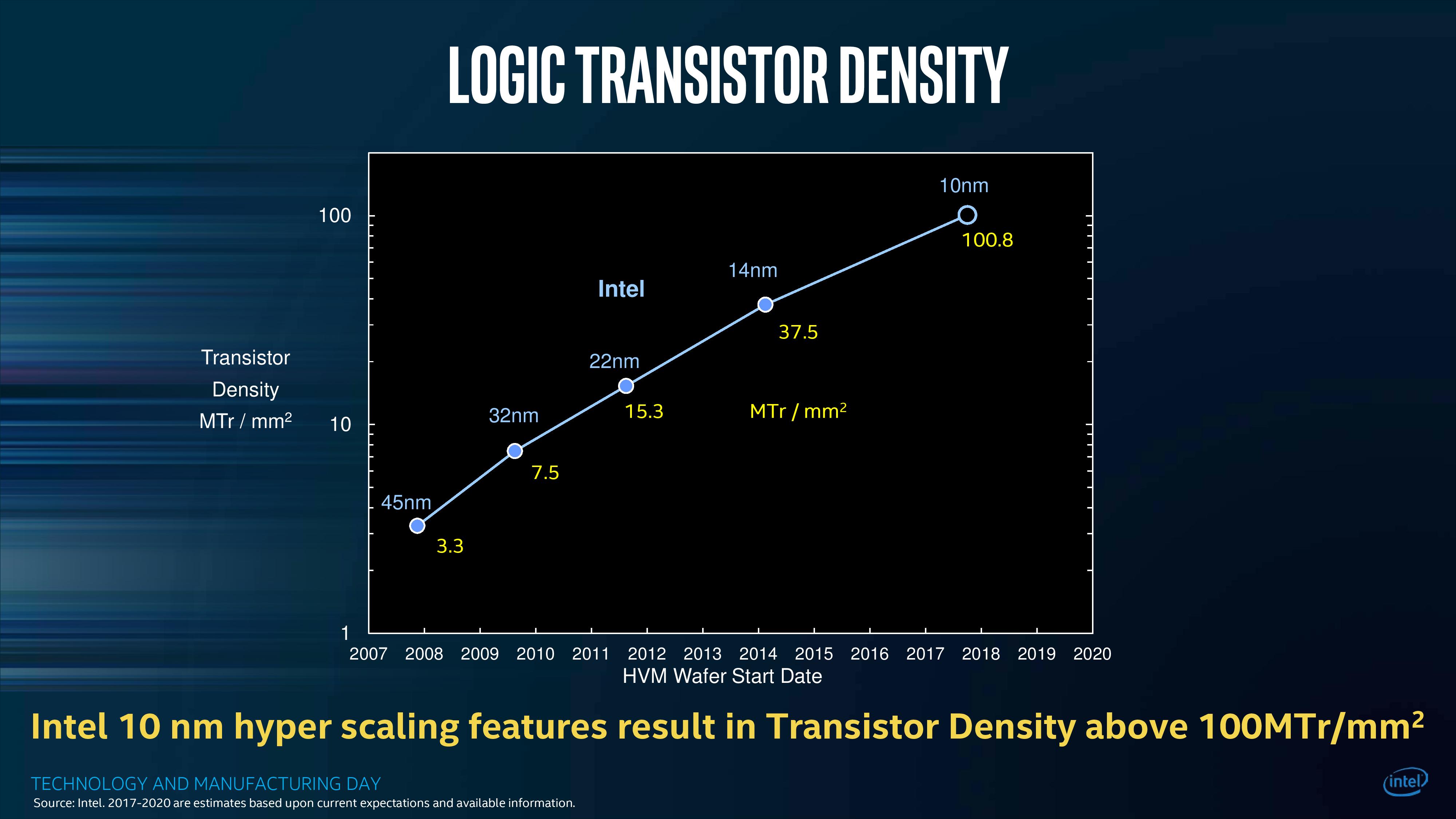
Back at Intel’s 2017 Technology and Manufacturing day, the company put out this slide, showing the millions of transistors per mm2 (MTr/mm2). This shows Intel making a very sizable 2.7x jump from 37.5 MTr/mm2 on its best 14nm node up to 100.8 MTr/mm2 on its 10nm node.
At the same time, Intel has suggested that the industry use a new way to measure transistor counts, based on the sizes of the two most common types of transistors in modern microprocessors.
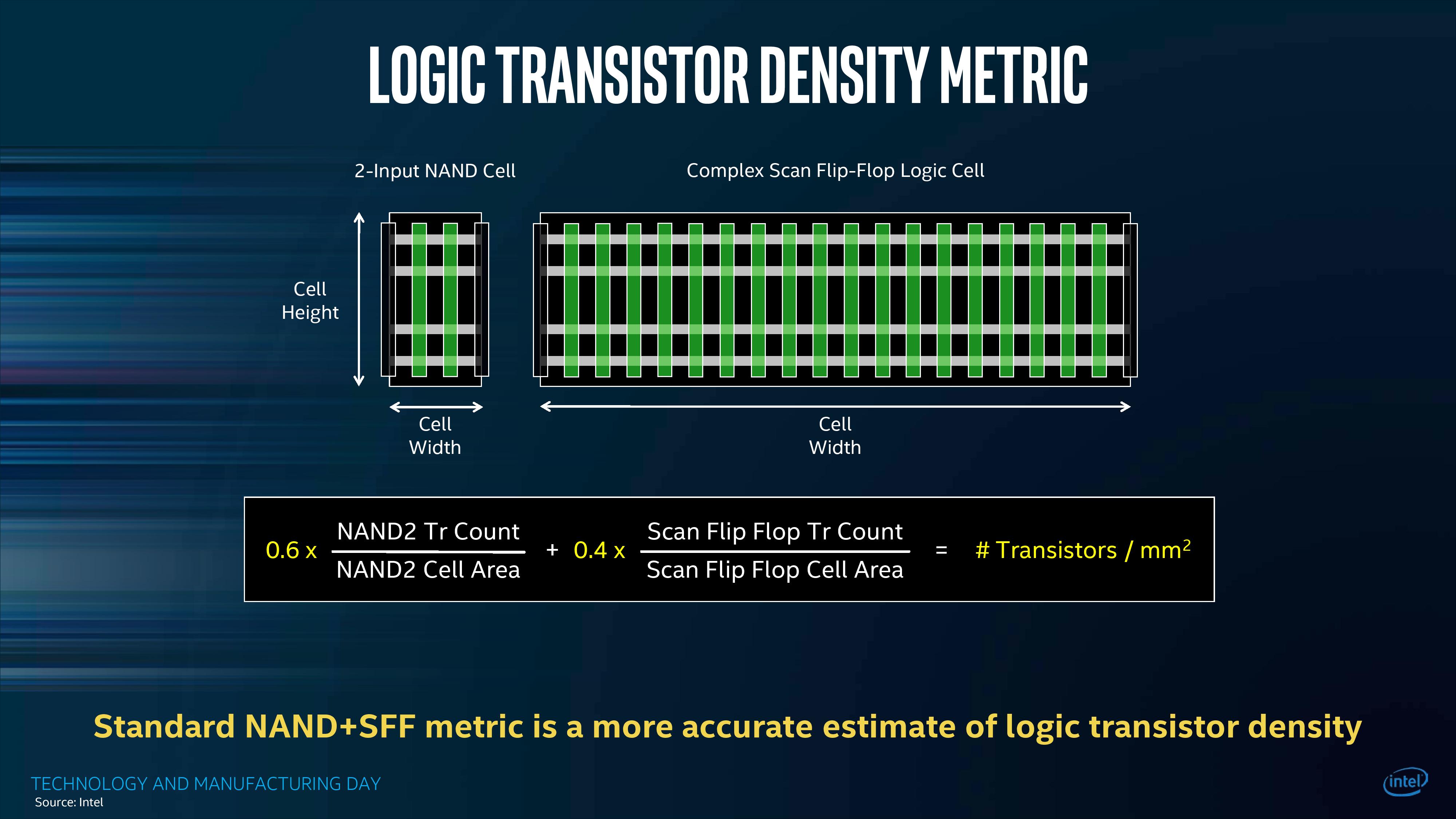
Under this metric, Intel wants the number of transistors per unit area to be divided into NAND2 cells and Scan Flip Flop Cells, and weight them 60/40 accordingly. This is how Intel gets to the 100.8 MTr/mm2 number.
However, at IEDM 2018, Intel presented some different numbers for older processes. They also went into detail about some of the numbers on Cannon Lake.
| Intel's Process Node Density | |||||||||
| 90 nm |
65 nm |
45 nm |
32 nm |
22 nm |
14 nm |
14 ++ |
10 nm |
7 nm* |
|
| Year | 2004 | 2006 | 2008 | 2010 | 2012 | 2014 | 2018 | 2019 | 2023 |
| Density MTr/mm2 |
1.45 | 2.08 | 3.33 | 7.11 | 16.5 | 44.67 | 37.22 | 100.76 | 237.18 |
| * Estimated | |||||||||
(The reason that 14nm++ is less dense than 14nm is that in order to improve frequency, Intel relaxed some of the design rules to allow for greater margins in design.)
Intel’s new method of counting adds a bit to Intel’s older processes, but 10nm stays where it is. This value, the company stated, is a combination of 90.78 MTr/mm2 for NAND2 gates and 115.74 MTr/mm2 for Scan Flip Flops.
There’s More To It
Intel also disclosed at IEDM that it has three types of logic libraries at 10nm, depending on the functionality required. These are short libraries (HD, high density), mid-height libraries (HP, high performance), and tall libraries (UHP, ultra-high performance). The shorter the library, the lower the power and the higher the density, however the peak performance is also lower. Ultimately the chip design is often a mixture of libraries – the shorter libraries work well for cost-sensitive applications, or for IO, and uncore. The larger libraries, by being less dense and having higher drive currents, are usually afforded for the most critical paths in the design.
The three libraries on Intel’s 10nm as a result come in three different densities. Only the high density library actually has the full 100.78 MTr/mm2:
| Intel 10nm Cell Libraries | ||||
| Name | Density MTr/mm2 |
Fins | Cell Height |
|
| HD | High Density | 100.78 | 8 | 272 nm |
| HP | High Performance | 80.61 | 10 | 340 nm |
| UHP | Ultra High Performance | 67.18 | 12 | 408 nm |
The reason why these cells differ in size is due to the number of fins in each cell, and thus fins per transistor. The number of fins adjusts the cell height, and additional fins allows more drive current for more performance, at the expense of power and area.
This graph from WikiChip shows the relationship between them for power and performance:
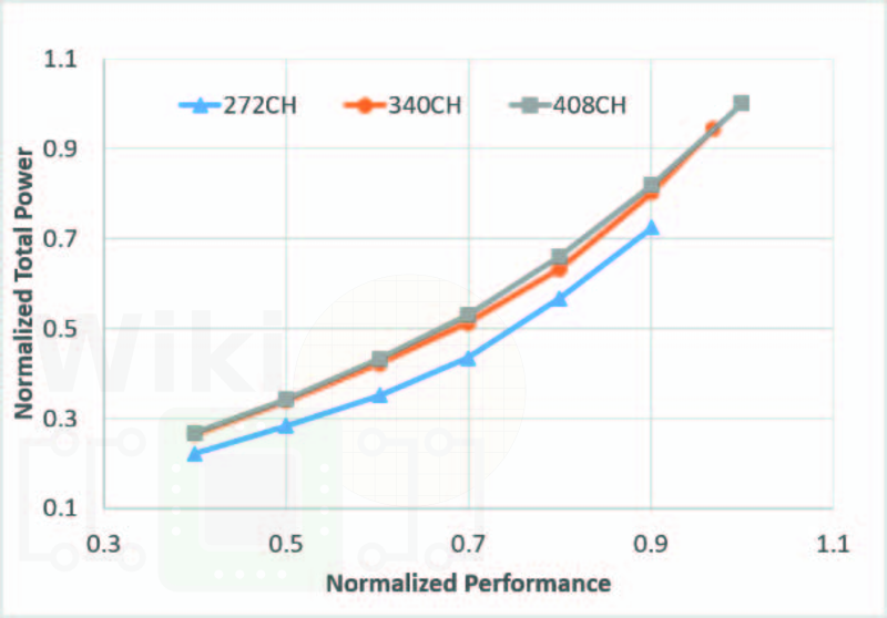
This makes a strong case for the HD cells for almost everything non-performance related, HP cells for most performance things, and UHP cells along the critical path. Ultimately the density that Intel uses from chip to chip is going to change depending on what cells they use and in what proportions. However within a specific chip design (say, a mid-core count Xeon), all chips built on that design will have the same cell layouts.
Fin Mechanics
In order to understand a lot of what Intel is doing at 10nm, we need to discuss fin, gate, and cell mechanics as well as define some terms relating to transistors and FinFETs. Starting with a diagram of a traditional FinFET:

The source-to-drain of a transistor is provided by a fin (in grey) going through a gate (in green) while imbedded in an oxide. The key metrics here are the fin height, the fin width, and the gate length. The idea is to make each of these as small as possible but still perform both at speed and as intended. During Intel’s 22nm the company used ‘tri-gate’ transistors that involve multiple fins together to increase total drive current for better performance.
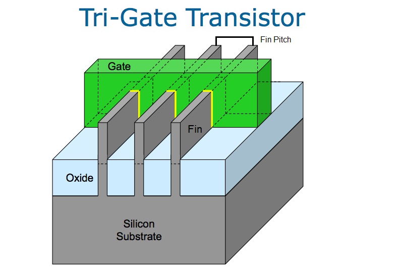
This introduces a new metric, the ‘fin pitch’, as the distance between fins. Similarly, if a fin passes through multiple gates, the distance between the gates is known as the ‘gate pitch’. Origianl diagrams come from Intel with our modifications.
In reality, we see images that look like this, showing the fins:
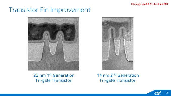
In this image Intel showed the improvement from 22nm to 14nm, with taller fin heights, smaller fin widths, and shorter fin pitches, with more of the peak of the fin imbedded into the gate.
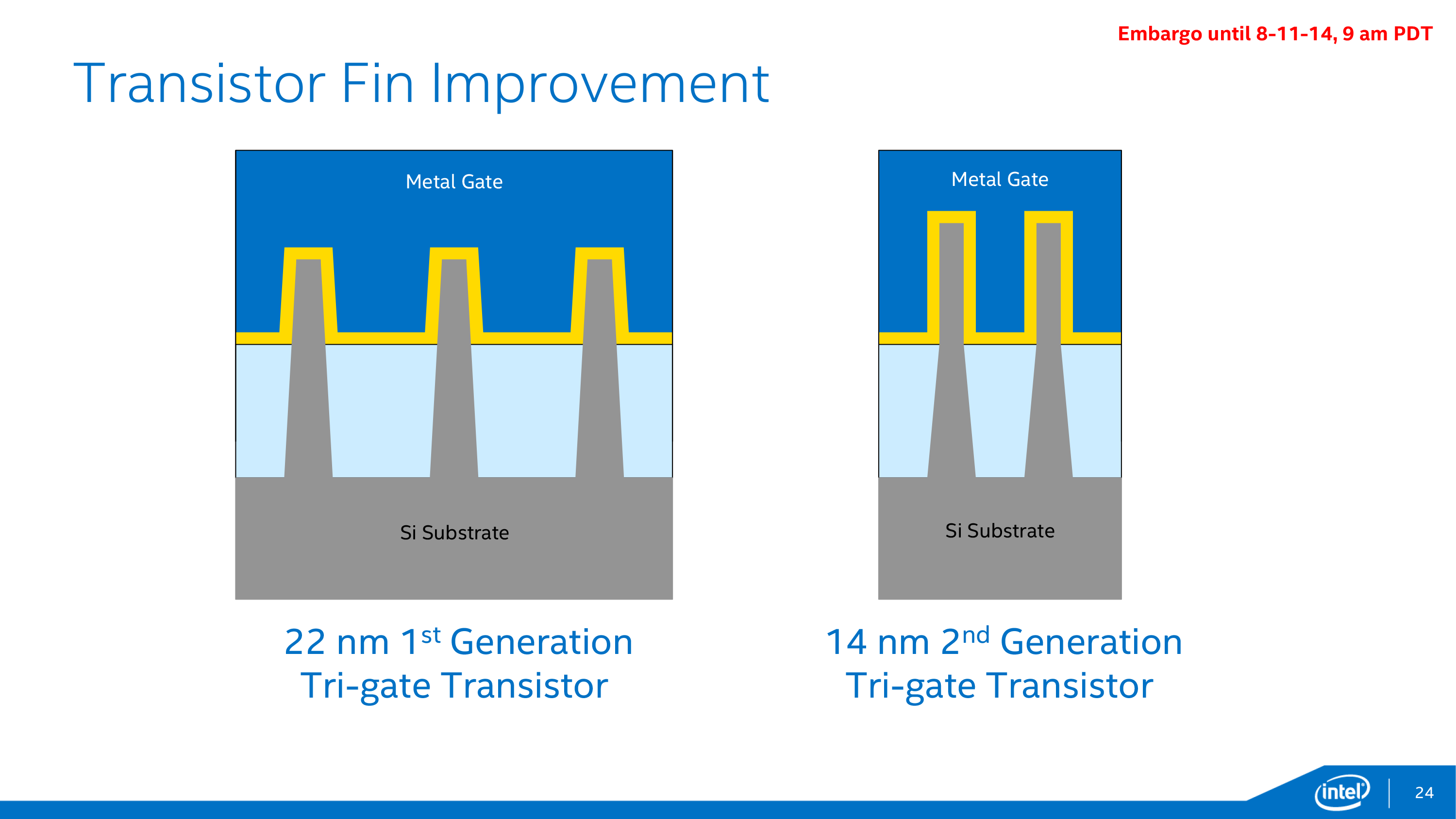
The more contact between the fin and metal gate, and the smaller the fin and fin pitch, the lower the leakage and the better the performance. It’s all a question of increasing drive current, but also managing stray capacitance and gate capacitance.
When it comes to 10nm, Intel is being aggressive in its fin design. Here are the basic numbers.
| Comparing Intel 14nm to Intel 10nm | |||
| 14nm | 10nm | Change | |
| Rated Density | 44.67 | 100.78 | 2.26 x |
| Fin Pitch | 42 nm | 34 nm | 0.81 x |
| Fin Width | 8 nm | 7 nm | 0.88 x |
| Fin Height | 42 nm | 43-54 nm | 1.02-1.29 x |
| Gate Length | 20 nm | 18 nm | 0.90 x |
| Contact Gate Pitch | 70 nm | 54 nm | 0.77 x |
| Minimum Gate Pitch | 52 nm | 36 nm | 0.69 x |
At IEDM 2017, Intel presented a fin height of 43 nm to 54 nm (officially, 46 nm), increased from 42 nm, with more contact between the fin and the gate. The fin height can be adjusted depending on the needs of the transistor. The fin width moves from 8nm down to 7nm, which means there is actually something in this process smaller than 10nm. The fin pitch needs to be small, to avoid parasitic capacitance, but the technology becomes more and more challenging to do this – for 10nm, Intel moves from a 42nm pitch to a 34 nm pitch, which is where its ability to do ‘Self-Aligned Quad Patterning’ (SAQP, more later) comes in.
I’m going to quote David from WikiChip here, who explains how this is done:
Adding more steps to the process naturally incurs a penalty in production time and a potential loss in yield.
The end result for the fins is a diagram that looks like this, showing Intel’s improvements from its first generation of FinFET technology:
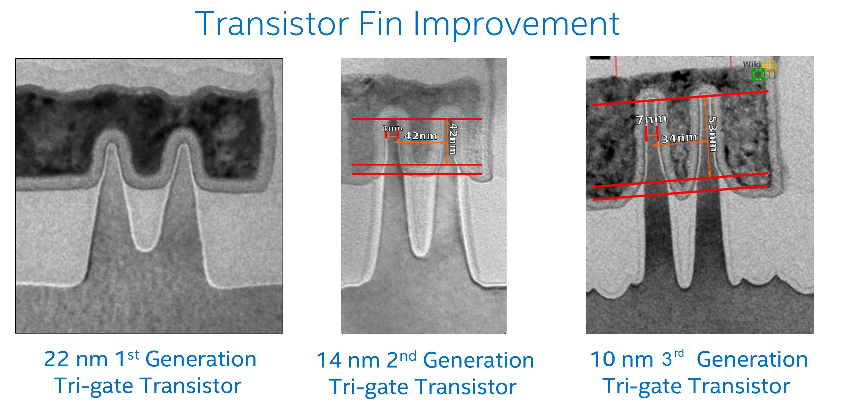
It doesn’t exactly look like much, but this is part of what it takes to drive new generations of semiconductor performance. At this scale, every nanometer counts. The fins are now more densely packed, and have more contact area with the gate. This helps with the drive current, the capacitance, and ultimately, density. Intel also improved the source and drain diffusion regions by adding a conformal titanium layer. The contact area between the fin and the trench (the grey bit under the gate) requires a lot of attention, with the idea to minimize contact resistance between the two. For 10nm, Intel changes this tungsten contact for a cobalt one, which according to the materials affords a 60% reduction in contact line resistance.
Building A Cell, and Managing Cell Size
A cell is a combination of a fixed number of fins with a varying amount of gates. Each cell has to connect ground and power at the top and bottom, which at a predefined position keeps it easier for routing and other analysis. Cells are almost like mix and match – multiple cells of a uniform height are laid in order, depending if the cell is for capping a logic cell, a logic cell itself, or voltage stability/isolation etc.
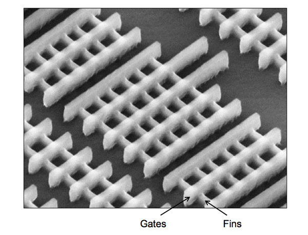
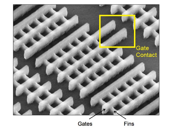
Here is an Intel SEM image from its 22nm process, showing cells with six fins and two fins, but varying lengths of gates.
Within each cell, there are active fins that pass current, and inactive fins that act as spacers. Intel’s highest density cell, HD, has a total of eight fins, however only five of which are active fins.
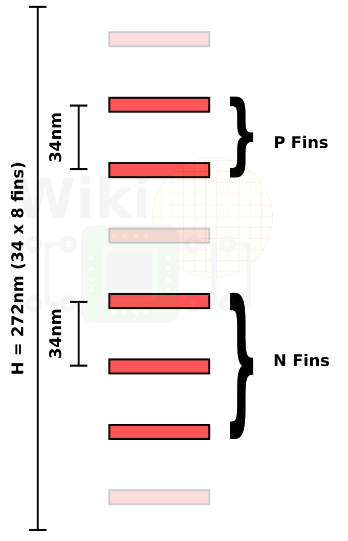
Image from WikiChip
These cells are used for cost-sensitive applications where density is required, or for non-high performance situations such as IO. With eight fins, this cell has two active ‘P’ fins and two active ‘N’ fins, with an optinonal additional active ‘N’ fin for various logic functions where prioritization is needed (such as NAND over NOR).
The other cell sizes that Intel uses, HP and UHP, have ten and twelve fins respectively. In each case there is one additional P fin and one additional N fin, both of which help provide additional drive current to aid peak performance at the expense of efficiency. The total height of the cell is the fin pitch (distance between fins) multiplied by the number of fins.
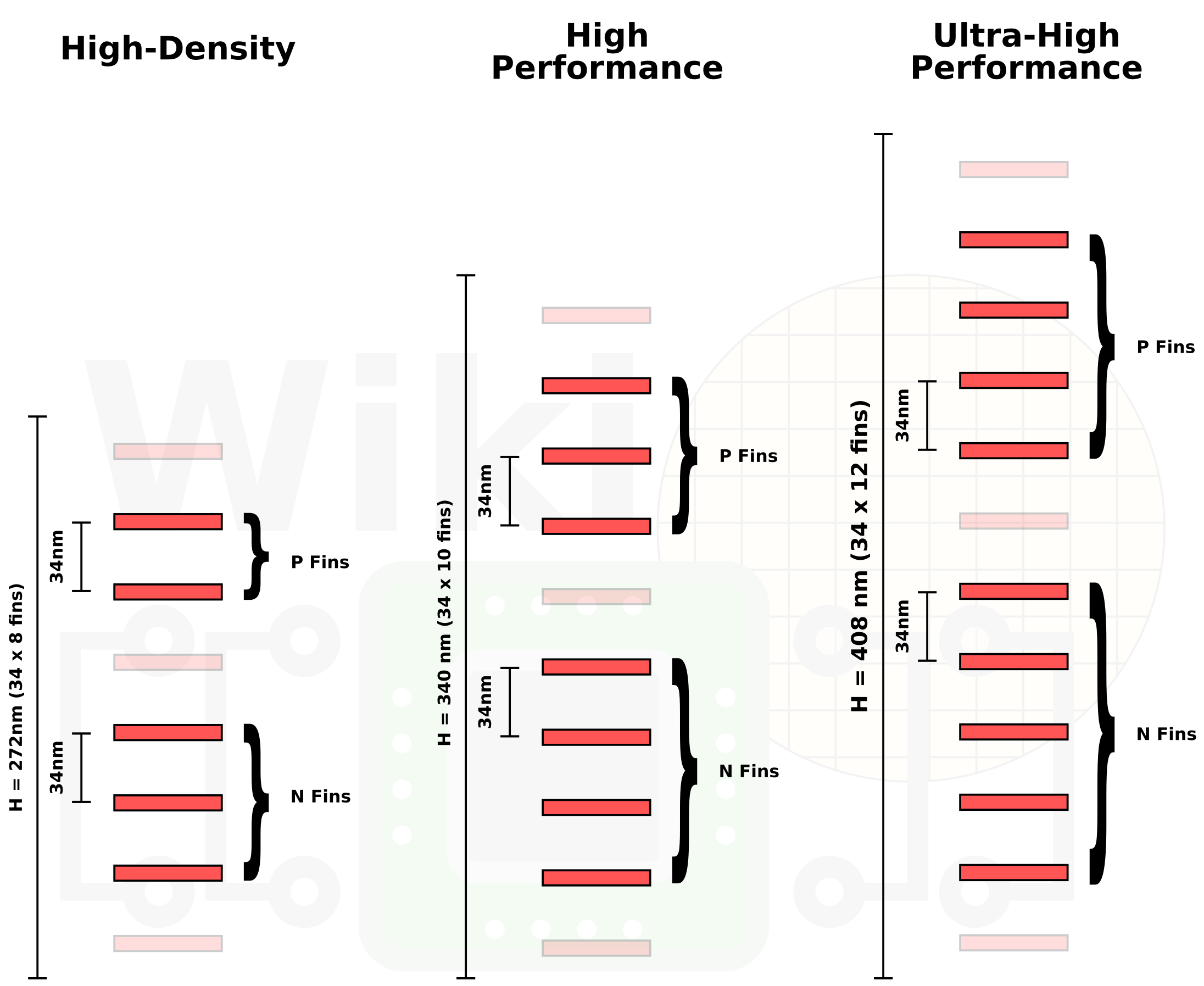
Image from WikiChip
It is worth noting that the faded out fins are usually present in the design, but are just dummy fins as part of the design.
One of the ways to measure density in this context is to multiply the Gate Pitch (or specifically, the Contact Poly Pitch) by the Fin Pitch (or Minimum Metal Pitch), known as the CPPxMMP metric. Because saying ‘10nm’ or ‘7nm’ has little bearing on the process at this point in history, this metric gives some idea of exactly how dense a process is.
| Comparing Different Process Nodes CPPxMMP |
||||||||||
| Intel | TSMC | Samsung | ||||||||
| CPP | MMP | CPP | MMP | CPP | MMP | |||||
| 28 nm | - | - | 117 nm | 90 nm | - | - | ||||
| - | 10530 nm2 | - | ||||||||
| 22 nm | 90 nm | 80 nm | - | - | - | - | ||||
| 7200 nm2 | - | - | ||||||||
| 16 / 14 nm | 70 nm | 52 nm | 90 nm | 64 nm | 78 nm | 64 nm | ||||
| 3640 nm2 | 5760 nm2 | 4992 nm2 | ||||||||
| 10 nm | 54 nm | 44 nm | 66 nm | 44 nm | 68 nm | 48 nm | ||||
| 2376 nm2 | 2904 nm2 | 3264 nm2 | ||||||||
| 7 nm | - | - | 54 nm | 40 nm | 56 nm | 40 nm | ||||
| - | 2160 nm2 | 2240 nm2 | ||||||||
From this metric, you would believe that TSMC’s 7nm amd Samsung's 7nm were both slightly denser than Intel’s 10nm. This is one reason why Intel wanted to change the way we define density into a mixture of cell sizes. But this metric doesn’t accurately reflect different cell libraries that use different heights (and thus a different number of fins per cell). However, cell size is not the only trick in the book.
Dummy Gates
Between cells there will often be a number of dummy gates used as spacers. In Intel’s 14nm designs, a cell would have a dummy gate at either end, meaning that between cells there would be two dummy gates. For the 10nm process, two adjacent cells can now share a single dummy gate.
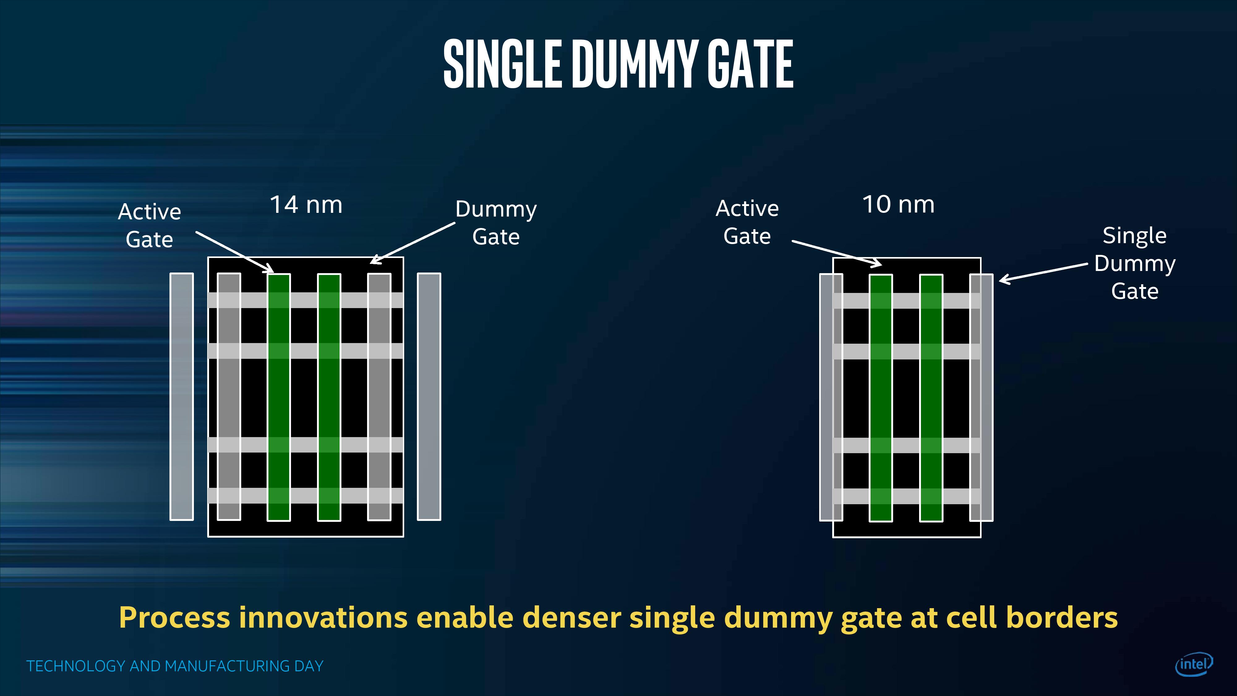
This mainly has density advantages, with Intel claiming a 20% area saving across a chip. Based on images that Intel showed at ISSCC, there isn’t actually a physical gate there, but actually a really deep trench.
Contact Over Active Gate (COAG)
Within a transistor, the gate contact is the control point where the current for the gate is applied to control between the source and the drain sides of the fin. Normally the gate contact is beyond the standard cell, as shown in this diagram:
This adds extra space to the x/y dimension, but is somewhat unavoidable. For 10nm, or at least the version currently in Cannon Lake, Intel is deploying a method called ‘Contact Over Active Gate’ (COAG) which places the gate contact over the cell.
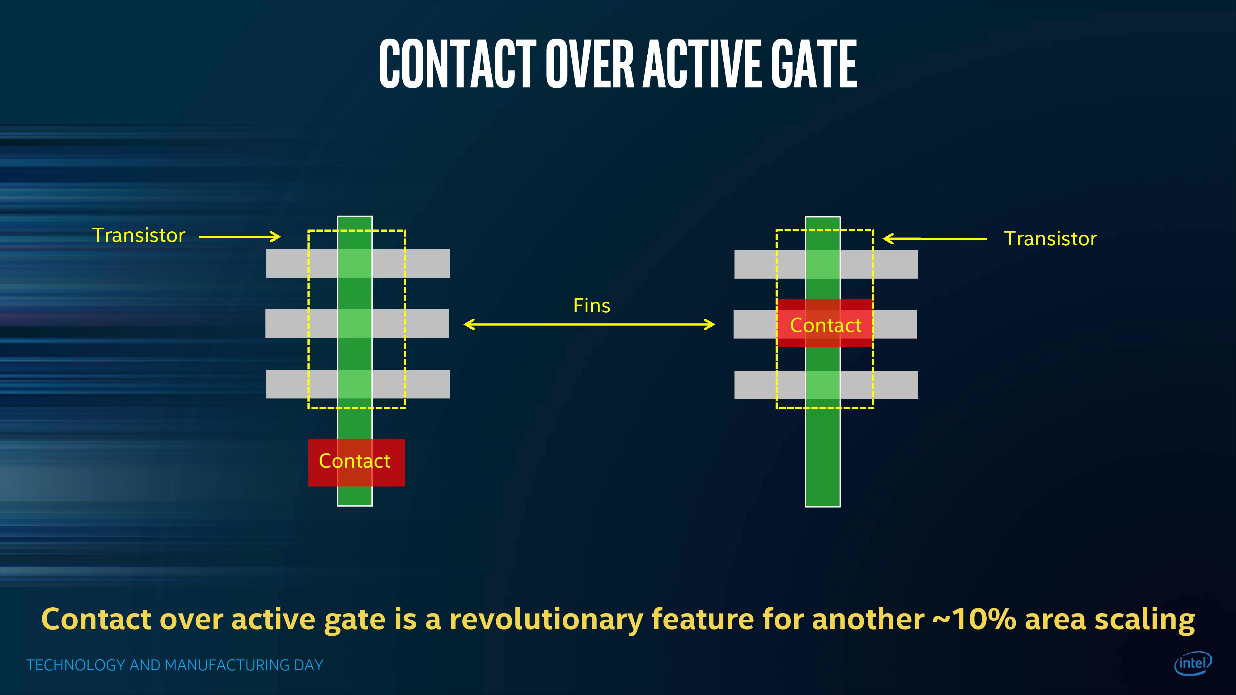
This is a complex change – the contact has to sit above the cell but not directly interfere with any of its properties. It adds several steps to the manufacturing process (one etch, one deposition, and one polish), but affords a potential ~10% better area scaling over the whole chip.
One of the reports about Intel’s 10nm process is that COAG is a risky implementation, and that while Intel has got it to work, it is not as reliable as expected due to relying on self-aligned diffusion to form a tight contact. Based on our discussions, the COAG design in Cannon Lake only seems to be working at low performance/low power, or at high performance/super-high power, which is at the ends of the spectrum but not in the middle. We expect Intel to mention how they’ve adjusted the design as and when they want to discuss an updated 10nm in detail.
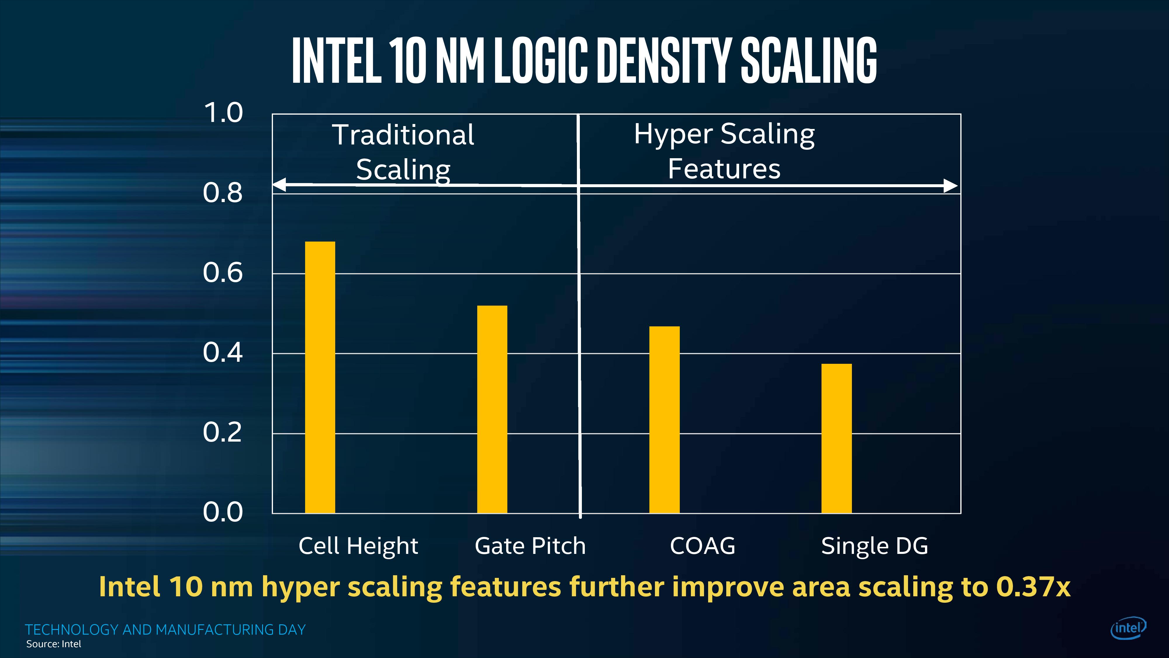
Overall, with the CPPxMMP adjustments, Dummy Gates, and COAG, Intel claims to have achieved a scaling factor of 0.37x over 14nm.
Applying Power Delivery: Double The Design Effort
In a standard cell design, power delivery is often managed by automated EDA tools. This is often a lot quicker than hand placement, improving time to market. However, in order to get the density improvements to work, Intel had to work with EDA tool vendors in order to apply power delivery both at the ‘block’ level, and for different cell alignments. This was an industry effort that afforded a number of optimizations.
A standard chip is built up as a series of metal layers to help deliver data and power. This series of metal layers is called the metallization stack, and forms part of the ‘back-end of line’ (BEOL) of how the chip is made, and can be independent of the transistor design.
Intel’s 10nm metal stack is 13 layers, one more than 14nm, and two more than 22nm. Intel’s official design rules for its metal stack are as follows
| Intel's 10nm Metal Stack | |||
| Layer | Metal | Pitch | Patterning |
| Fin | 34 nm | Quad | |
| Gate | Copper / Cobalt | 43-54 nm | Dual |
| Metal 0 | Cobalt | 40 | Quad |
| Metal 1 | Cobalt | 36 | Quad |
| Metal 2, 3, 4 | Copper | 44 | Dual |
| Metal 5 | Copper | 52 | Dual |
| Metal 6 | Copper | 84 | Single |
| Metal 7, 8 | Copper | 112 | Single |
| Metal 8, 10 | Copper | 160 | Single |
| Thick Metal 0 | Copper | 1080 | Single |
| Thick Metal 1 | Copper | 11000 | Single |
Cobalt is a ‘barrier-less’ conductor, which means that compared to copper it does not need a barrier layer between wires, plus it also scales down further than copper, providing more beneficial characteristics at smaller sizes. TechInsights also reports detecting Ruthenium in the lower layers on their Cannon Lake processor, however Intel has not mentioned it in its disclosures.
Dealing with placing wires on each layer is different to building fins and trenches, which is why the pitch changes through the stack. However joining the metal power rails in the right way is an important requirement in design. The power stubs of each cell are typically found on the corners, connecting the cell to the Metal 2 layer through the Metal 1 layer. As a result, the stubs are thought of being at the ‘cell level’. Intel has changed this and moved the power stubs to the ‘block level’, by identifying common groups of cells and placing them at optimum positions.
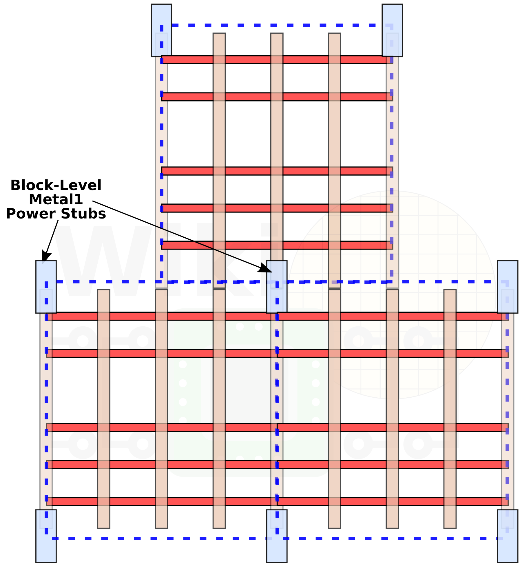
Image from WikiChip
This is not a trivial change. It hasn’t been possible until Intel’s 10nm to do with the automated EDA tools – it was possible by hand, but that increases the design time of the chip. The step Intel made with the EDA tool makers is to develop ‘block aware’ automation, so this can happen fully inside the tools. This also allows the Metal 1 layer to be less densely populated, which actually helps with cell level density.
It should be noted that in order for this to work, the gate pitch in the cell and the Metal 1 layer pitch needs to align. As shown in the table above, the Gate pitch is 54nm, while the M1 pitch is only 36nm, which isn’t equal. While it is not equal, it is in a 3:2 whole ratio. This whole ratio means that while there is a potential for misalignment, it happens at the block level. The EDA tools have to deal with this, usually by adding in spacers, which reduces density. To get around this, Intel duplicated its entire cell library for two formats: for cells with misaligned contacts and for cells with aligned contacts. This means that the if EDA placement tools know that two different versions exist, it can use the version required depending on the location, ultimately saving density without having to use gaps. Being ‘alignment aware’ was a significant step for both Intel to create two versions of every cell but also for the tools to implement this feature. The alignment aware feature has repercussions through the metal stack, and Intel stated that depending on the cell density this could give another 5-10% density improvement. Not bad for double the work (!).
It should be stated that Intel calls this ‘a solved problem’, and we are expecting the company to use it in all products going forward where the pitch mechanics make it applicable.
Scaling Wires
Going smaller with wires has one significant issue: resistance. Having a lower cross-sectional area for electrons to travel through means that they are cramped into a smaller space, resulting in an increased resistance, and relationship between the two is inversely proportional.

The resistance of the wire is the resistivity (a function of the metal) multiplied by the length divided by the cross-sectional area. So ideally as area decreases, using a metal with a lower resistivity helps a lot. Otherwise, additional drive current is needed, which has other knock-on effects such as electromigration.
So at this time Intel is moving from Copper to Cobalt for its thinnest wires in the lower metal layers. The thing is, the resistivity of Cobalt is actually higher than that of Copper, almost four times as much. The reason why Copper gets the nod is two things – scaling, and electomigration.
Electromigration is when the high-speed electrons knock metal atoms out of their spots in the metal structure by momentum transfer. Normally this isn’t an issue, however as the current increases and the cross sectional area decreases, and more electrons are present, this can become a concern. The more atoms out of place, the higher the resistance of the wire, until there is a complete disconnect. Electromigration happens more often at grain boundaries in the metal, and when the average mean free path is long. A circuit that fails due to electromigration cannot be repaired.
A lot of effort is put into controlling electromigration, and EDA tools are automatically designed to mitigate against it. This means adding in diffusion barriers and liners, which add to the overall wire placement dimensions. However, these liners do not scale as much as the wire does.

Yet another awesome image from Wikichip.
So when a copper wire is given as a certain value for its width, part of that is taken up by these diffusion barriers and liners, meaning that the actual cross section of copper is a lot lower, and as we scale down, much, much lower.
This is where cobalt wins over copper, in several areas in fact. While the resistivity of cobalt is 4x higher, the nature of cobalt means that the diffusion barriers need only be 1nm, allowing for more of the wire volume to be bulk cobalt. This allows cobalt to scale down to much smaller wire widths. The mean free path is shorter, down from 40nm to sub-10nm, meaning that electomigration is less of an issue.
Obviously cobalt isn’t used for everything; when the wire widths are wide enough, then the traditional copper implantation is a tried and tested method with lower resistivity which wins the day (the gain in area from cobalt doesn’t offset the resistivity disadvantage). For the layers where it matters, particularly M0 and M1, Intel states that cobalt affords a 2x reduction in layer-to-layer resistance (via resistance) and a 5-10x improvement in electromigration within the layers.
As David from Wikichip points out, in future node advancements, as more and more layers go over the cobalt-copper crossover point, we will start to see cobalt move up the stack. Or, as Techinsights found, Ruthenium might be making itself known in some layers.
Putting It All Together
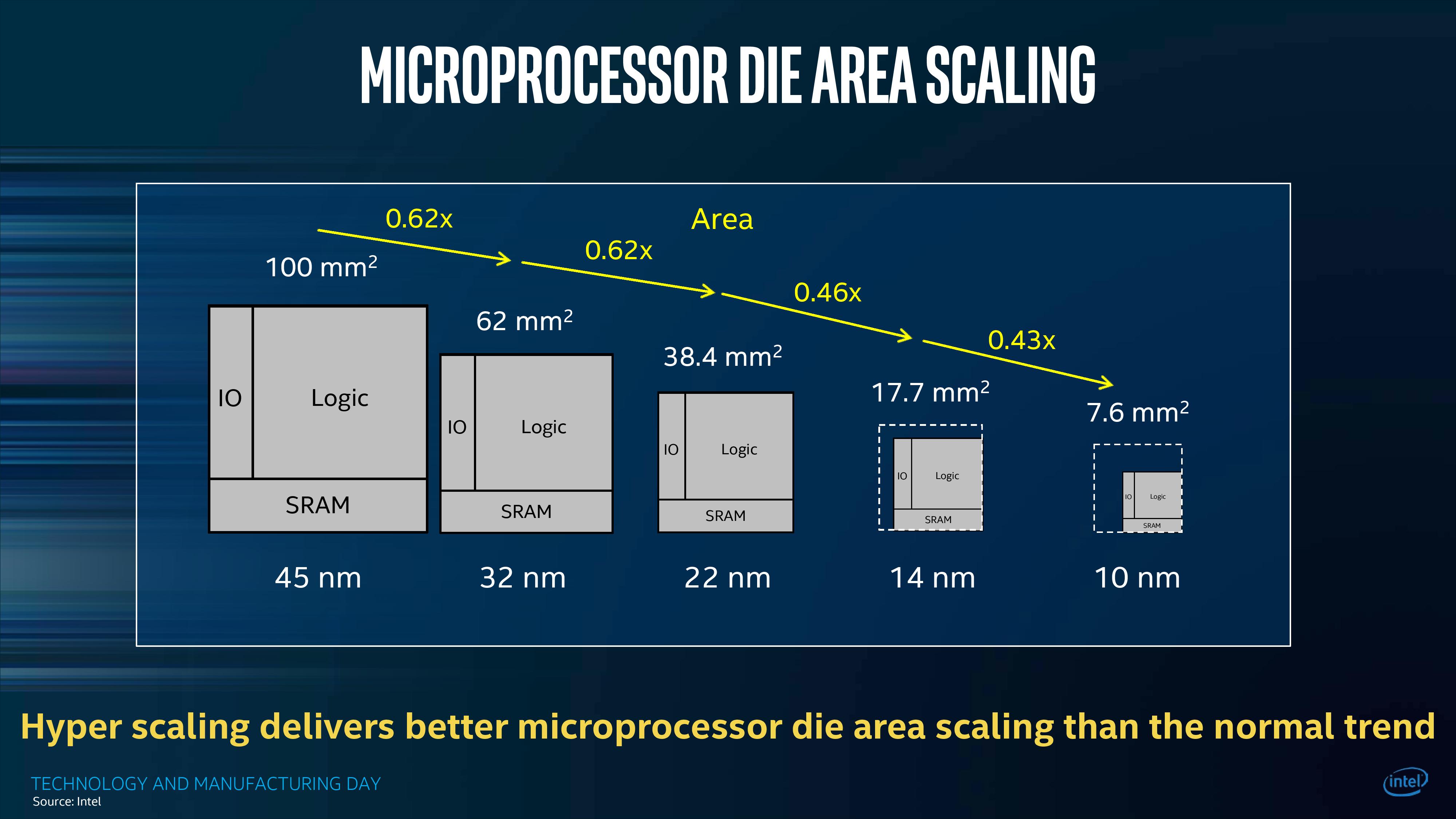
Back at the beginning, we mentioned that Intel’s key metric on its 10nm process is meeting the 100 million transistors per square millimeter mark. This is for its high density cell libraries, rather than for its ultra-high-performance cell libraries, but it is still an impressive feat nonetheless. When approaching this sort of scaling, every area needs to be improved – 10% here, 15% there, another 10% somewhere else, and it all adds up. At Intel’s Technology and Manufacturing Day at 2017, Intel stated that for a given chip design on 45nm, what would have taken 100 square millimeters then can now fit into 7.6 square millimeters today.
What is interesting to note is the slide that appeared in this deck only two clicks later, discussing the capacitance and performance of Intel’s planned generations of 10nm.
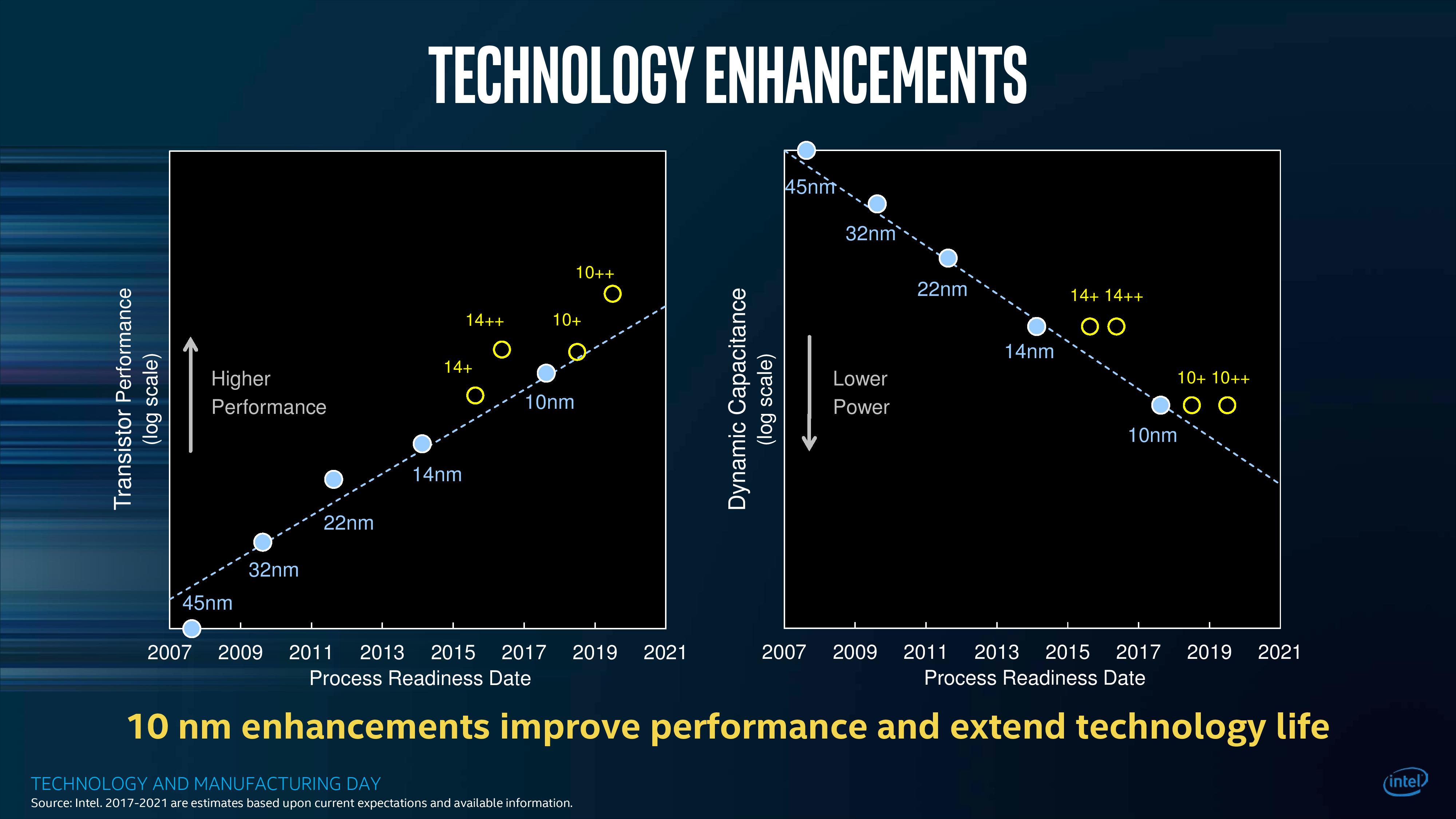
On the right, Intel shows that every version of 10nm in its pipeline has a lower dynamic capacitance than 14nm, which is a good thing. However, in terms of transistor performance on the graph on the left, both 10nm and 10nm+ have a lower transistor performance than the latest version of 14nm++.
For reference, Cannon Lake is on what Intel calls its ‘10nm’ process node. Ice Lake, the product destined for consumer devices at the end of 2019 (in 8-10 months from now), is on the ‘10nm+’ process node. This means that the products in December 2019 will still be behind in transistor performance to the products launched in October 2017. The new chips will have some benefits, such as power and new microarchitectures, but this is worth noting what Intel has already stated to the press and investors.
Sources. Well Worth The Read
[1] https://fuse.wikichip.org/news/525/iedm-2017-isscc-2018-intels-10nm-switching-to-cobalt-interconnects/
[2] https://fuse.wikichip.org/news/2004/iedm-2018-intels-10nm-standard-cell-library-and-power-delivery/
[3] https://fuse.wikichip.org/news/1371/a-look-at-intels-10nm-std-cell-as-techinsights-reports-on-the-i3-8121u-finds-ruthenium/
[4] https://techinsights.com/technology-intelligence/overview/latest-reports/intel-10-nm-logic-process/
[5] https://www.anandtech.com/show/8367/intels-14nm-technology-in-detail


129 Comments
View All Comments
BigMamaInHouse - Friday, January 25, 2019 - link
Thank you for your Great reviews.Look like we should not ecpect much from those new 10nm CPU's for cunsumers for new future, maybe in Q1 2020 with 10++ gen.
2019 going to be on AMD's Favor!.
jaju123 - Friday, January 25, 2019 - link
12 or 16 core Ryzen with a 13% IPC increase, at equivalent power to the i9-9900k is not going to go well for Intel. Seems like they'll be able to compete with the AMD processors of 2019 around late 2020 at the earliest.ZolaIII - Friday, January 25, 2019 - link
Take a look at the Spec 2006 benchmark and make the comparation to A76 (Snapdragon 855) it beats this Intel SKU (@2.2 GHz) In most cases with only half the power used. When SVE NEON SIMD lies in CISC is doomed.Gondalf - Friday, January 25, 2019 - link
Unfortunately we don't know how perform AMD new cpus, only cherry picked results nothing more.Even less we know about power consumption. Are we certain AMD 7nm cores will are winner over 12nm ones?? AMD is unhappy about clock speed for example, so the IPC advantage will be likely vanished.
IMO AMD is painting a too bright future to be trusted. TSMC process is not perfect at all, instead of Nvidia should be on it right now.
levizx - Saturday, January 26, 2019 - link
Rubbish written in garbled words.KOneJ - Sunday, January 27, 2019 - link
What exactly are you trying to babble about here?Valantar - Sunday, January 27, 2019 - link
Lying about future products is grounds for lawsuits from shareholders (and possible criminal charges many places), so that's quite unlikely. We do have one indication of power draw from Zen2, from the live Cinebench demo where an 8-core Zen2 chip matched the 9900K's score at ~50W lower power. Of course we don't know how clocks will scale, nor the clock speed that test was run at, and it's relatively well established that Cinebench is a workload where AMD does well. Still, TSMC 7nm is proven good at this point, with several shipping large-scale SKUs on it (Apple A12, A12X, among others). Even if these are all mobile low-power chips, they're very high performance _and_ low power, which ought to fit Zen2 well. Also, the Cinebench score matching the 9900K means that either IPC has improved massively, SMT scaling on Zen2 is ~100%, or clocks are quite high. Likely it's a mix of all three, but they wouldn't reach that score without pretty decent clocks.Samus - Thursday, January 31, 2019 - link
Ignoring any Zen IPC improvement whatsoever, process improvements alone this year would make them competitive with Intel going forward. All they need to do is ramp up the clock frequency a bit without a TDP penalty and they have an automatic win...Makste - Saturday, March 6, 2021 - link
Lol😆Vegajf - Friday, January 25, 2019 - link
Icelake desktop will be out 3q 2020 from what I hear. We will have another 14nm refresh before then though.