Intel's 10nm Cannon Lake and Core i3-8121U Deep Dive Review
by Ian Cutress on January 25, 2019 10:30 AM ESTConclusion: I Actually Used the Cannon Lake Laptop as a Daily System
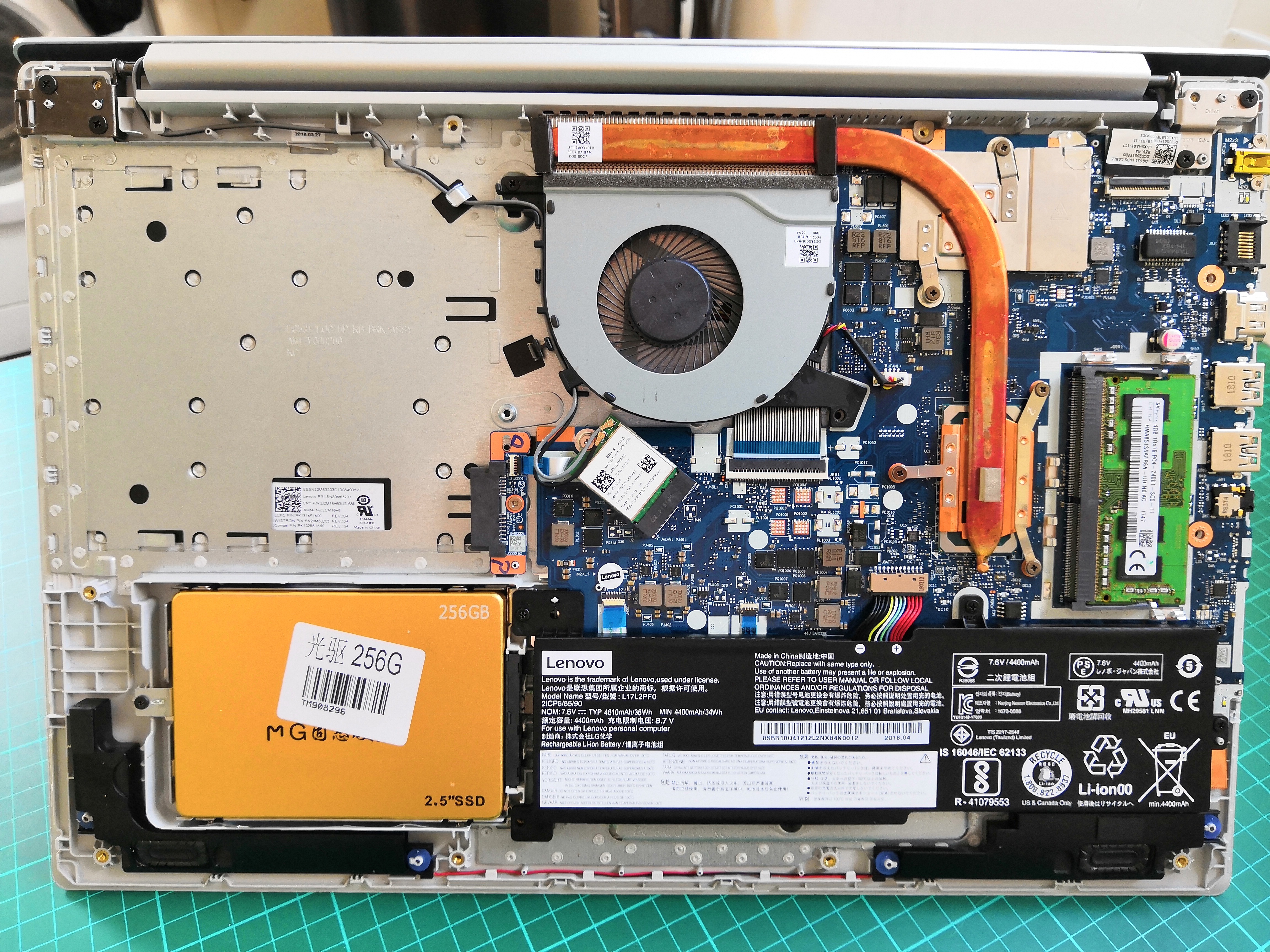
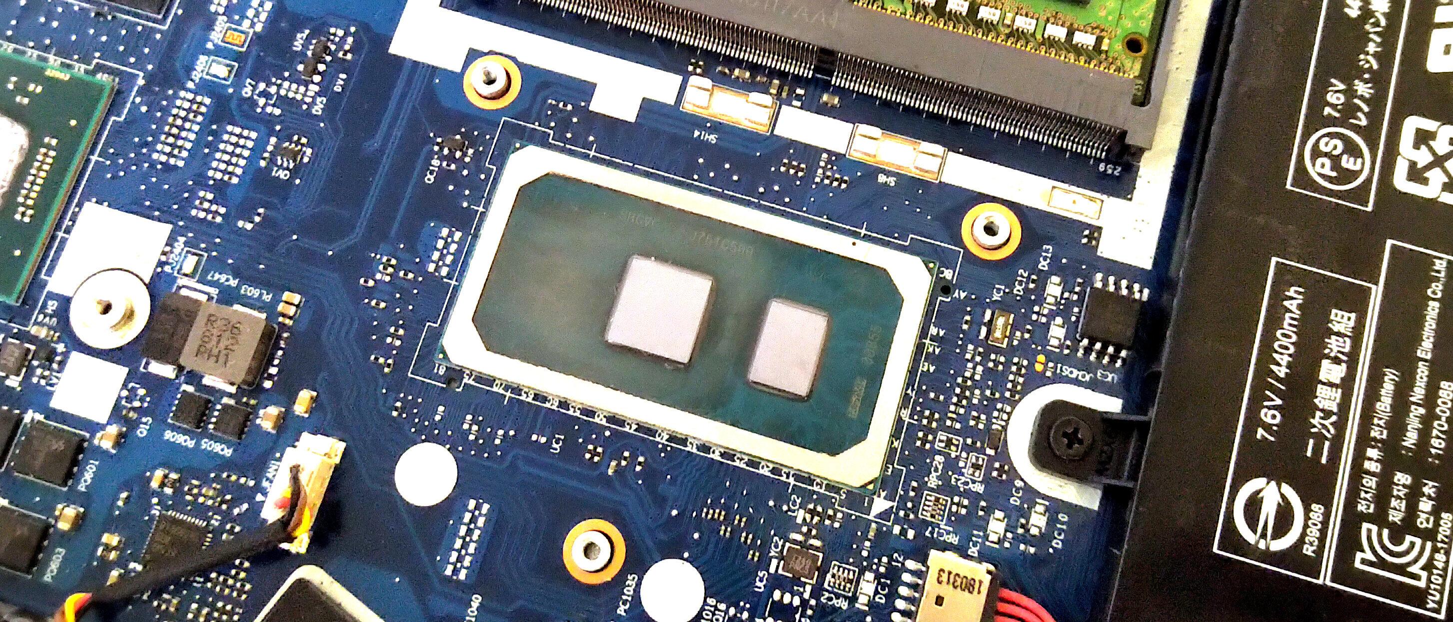
When we ordered the Lenovo laptop, not only was I destined to test it to see how well Intel’s 10nm platform performs, but I also wanted to see what the device was like to actually use. Once I’d removed the terrible drives it came with and put in a 1TB Crucial MX200 SSD, I started to put it to good use.
The problem with this story is that because this is a really bad configuration of laptop, it gives the hardware very little chance to show its best side. We covered this in our overview of Carrizo several years ago, after OEM partners kept putting chips with reasonable performance into the worst penny pinching designs. The same thing goes with this laptop – it is an education focused 15.6-inch laptop whose screen is only 1366x768, and the TN panel’s best angle to view is as it is tilted away from you. It is bulky and heavy but only has a 34 Wh battery, whereas the ideal laptop is thin and light and lasts all day on a single charge. From the outset, using this device was destined to be a struggle.
I first used the device when I attended Intel’s Data Summit in mid-August. On the plane I didn’t have any space issues because I had reserved a bulkhead economy seat, however after only 4 hours or so of light word processing on a low screen brightness, I was already out of battery. Thankfully I could work on other things on my second laptop (always take two laptops to events, maybe not day-to-day at a show, but always fly with two). At the event, I planned to live blog the day of presentations. This means being connected online, uploading text, and being of a sufficient brightness to see the screen. After 90 minutes, I had 24% battery left. This device has terrible battery life, a terrible screen, is bulky, and weighs a lot.
I will say this though, it does have several positives. Perhaps this is because the RX540 is in the system, but the Windows UI was very responsive. Now of course this is a subjective measure, however I have used laptops with Core i7 and MX150 hardware that were slower to respond than this. It did get bogged down when I went into my full workflow with many programs, many tabs, and many messaging software tools, but I find that any system with only 8GB of memory will hit my workflow limits very quickly. On the natural responsiveness front, I can’t fault it.
Ultimately I haven’t continued to use the laptop much more – the screen angle required to get a good image, the battery life, and the weight are all critical issues that individually would cause me to ditch the unit. At this price, there are plenty of Celeron or Atom notebooks that would fit the bill and feel nicer to use. I couldn’t use this Ideapad unit with any confidence that I would make it through an event, either a live blog or a note taking session, without it dying. As a journalist, we can never guarantee there will be a power outlet (or an available power outlet) at the events we go to, so I always had to carry a second laptop in my bag regardless. The issue is that the second laptop I use often lasts all day at an event on its own.
Taking Stock of Intel’s 10nm Cannon Lake Design
When we lived in a world with Intel’s Tick Tock, Cannon Lake would be a natural tick – a known microarchitecture with minor tweaks but on a new process node. The microarchitecture is a tried and tested design, as we now have had four generations of it from Skylake to Coffee Lake Refresh, however the chip just isn’t suitable for prime time.
Looking at how Intel has presented its improvements on 10nm, with features like using Cobalt, Dummy Gates, Contact Over Active Gates, and new power design rules, if we assume that every advancement works perfectly then 10nm should have been a hit out of the gate. The problem is, semiconductor design is like having 300 different dials to play with, and tuning one of those dials causes three to ten others to get worse. This is the problem Intel has had with 10nm, and it is clear that some potential features work and others do not – but the company is not saying which ones for competitive and obvious reasons.
At Intel’s Architecture Day in December, the Chief Engineering Officer Dr. Murthy Renduchintala was asked if the 10nm design had changed. His response was contradictory and cryptic: ‘It is changing, but it hasn’t changed’. At that event the company was firmly in the driving seat of committing to 10nm by the end of 2019, in a quad core Ice Lake mobile processor, in a new 3D packaging design called Lakefield, in an Ice Lake server CPU for 2020, and in a 5G/AI focused processor called Snow Ridge. Whatever 10nm variant of the process they’re planning to use, we will have to wait and see.
I’ll go back to this slide that Intel presented back at the Technology and Manufacturing Day:
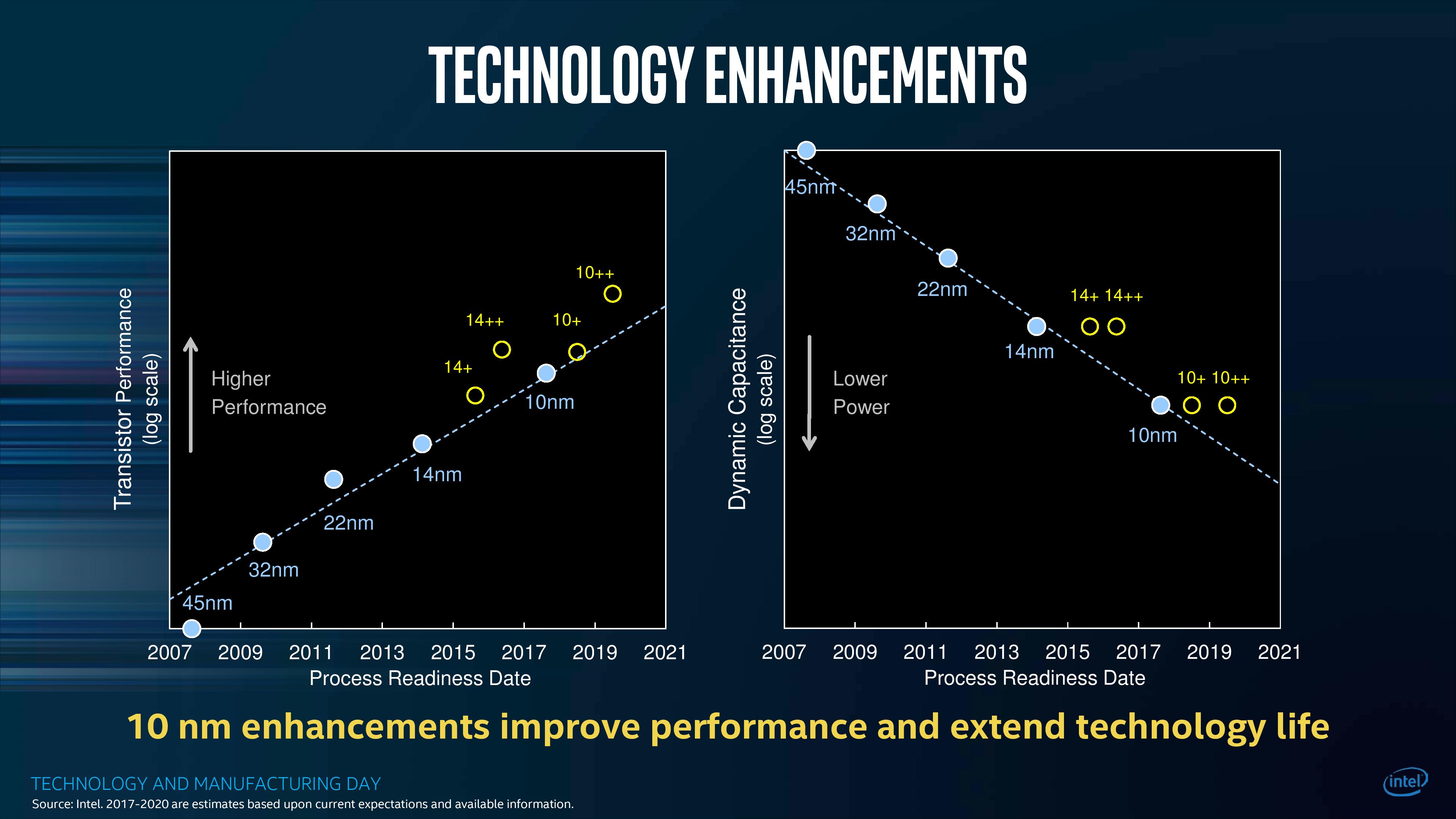
In this slide it shows on the right that 10nm (and its variants) have lower power through lower dynamic capacitance. However, on the left, Intel shows both 10nm (Cannon Lake) and 10nm+ (Ice Lake) as having lower transistor performance than 14nm++, the current generation of Coffee Lake processors.
This means we might not see a truly high-performance processor on 10nm until the third generation of the process is put into place. Right now, based on our numbers on Cannon Lake, it’s clear that the first generation of 10nm was not ready for prime time.
Cannon Lake: The Blip That Almost Didn’t Happen
We managed to snap up a Cannon Lake chip by calling in a few favors to buy it from a Chinese reseller who I’m pretty sure should not have been selling them to the public. They were educational laptops that may not have sold well, and the reseller just needed to get rid of them. Given Intel’s reluctance to talk about anything 10nm at CES 2018, and we find that the chips ‘shipped for revenue’ end up in a backwater design like this, then it would look like that Intel was trying to hide them. That was our thought for a good while, until Intel announced the Cannon Lake NUC. Even then, from launch announcement to being at general retail took four months, and by that time most people had lost interest.
At some point Intel had to make good on its promises to investors by shipping something 10nm to somewhere. Exactly how many chips were sold (and to whom) is not discussed by Intel, but I have heard some numbers flying around. Based on our performance numbers, it’s obvious why Intel didn’t want to promote it. On the other hand, at least being told about it beyond a simple sentence would have been nice.
After testing the chip, the only way I’d recommend one of these things is for the AVX512 performance. It blows everything else in that market out of the water, however AVX512 enabled programs are few and far between. Plus, given what Intel has said about the Sunny Cove core, that part will have it instead. If you really need AVX512 in a small form factor, Intel will sell you a NUC.
Cannon Lake, and the system we have with it inside, is ultimately now nothing more than a curio on the timeline of processor development. Which is where it belongs.


129 Comments
View All Comments
yeeeeman - Saturday, January 26, 2019 - link
As someone said it earlier in this thread, I think we miss opportunities when moving to a new process every two years. The mishap that Intel had just showed us how much better a process can become if you give the time to your engineers. 14nm started late, with some low clocked parts. We had some Broadwell chips that ran at 3.3 base. Then, Skylake came and the 6700k brought 4ghz at quite high power. Then, the 7700k came and another tweak to the process improved clocks, so we now got 4.7 GHz boost. After this, things moved up in core counts (which should've happen a long time ago, but with competition...) and we got 8700k and now 9900k with turbo to 5ghz. Until now, only 32nm with Sandy Bridge came close to 5ghz mark. Now, with a lot of time to tweak, they have become so confident in the 14nm process that they released a 5ghz stock cpu. Financials say the true story. Even if we cry about 10nm, truth is that things can move forward without a new process. It is cheaper actually to prolong the life of a certain process and if they can add enough improvements from generation to generation, they can afford to launch new process once every 4-5 years.Dodozoid - Saturday, January 26, 2019 - link
Indeed, we probably have to get used to a lot of +++ processes. During the architecture day, the new Intel people (old AMD people) mentioned they are decoupling the architecture from the process. That means they can make progress other than pushing clocks on the same core over and over, but IPC as well...KOneJ - Sunday, January 27, 2019 - link
Unfortunately, SB-derivatives seem to be needing a significant overhaul. "tocks" of late haven't exactly brought meaningful IPC gains. Hopefully deeper and wider *Cove designs are a step in the right direction. I just don't like that Intel seems to be taking an approach not dissimilar to the Pentium 4 the last time AMD reared its head. Only this time, a major departure in micro-architecture and steady process advantage isn't in the wings. Even with the *Coves, I think AMD may be able to build enough steam to solidly overtake them. There's no reason that Zen 4 and on couldn't go deeper and wider too, especially looking at power consumption on the front and back ends of the Zen core versus the uncore mesh. I think Zen derivatives currently will try the wider first. It actually might make the high core-count parts significantly more power efficient. Also could easily scale better than post-SB did if Agner Fog's analysis is anything to go by. Multiple CPU die masks and uncore topologies incoming? Wouldn't surprise me.dgingeri - Saturday, January 26, 2019 - link
Well, yeah, they can be improved upon over time, but that doesn't cut the production costs like a process reduction does. improving the process can increase yields and increase performance, but only by a limited percent. A process reduction increases the number of chips from a wafer by a much higher amount, even if there are more defects.Well, that was the way it worked up until the 14nm process.
With 10nm at Intel, they had far too many defects, and the process failed to give the returns they wanted for quite a while. That had as much to do with the quality of the wafers before production as it did the production process itself. They had to push the wafer producers to higher levels of purity in order to fix that. I'm fairly sure TSMC would have had the same issues with their 7nm, but Intel had already pushed the wafer production to higher levels of purity because of their problems, so TSMC was able to take a couple extra steps ahead because of that.
These days, we're going to see each step smaller take longer and longer to get right, because of these same hurdles. As things get smaller, impurities will have a higher and higher impact on production. We may not get as far as some are hoping, simply because we can't get silicon as pure as necessary.
name99 - Saturday, January 26, 2019 - link
"Another takeaway is that after not saying much about 10nm for a while, Intel was opening up. However, the company very quickly became quiet again."The history page is great. But I have to wonder if the ultimate conclusion is that the best thing, for both Intel and the world, is that they STICK to the STFU strategy? And that journalist stick to enforcing it.
One thing that's incredibly clear from all this is that Intel are utterly lousy at forecasting the future. Maybe it's deliberate lies, maybe it's just extreme optimism, maybe it's some sort of institutional pathology that prevents bad news flowing upward?
Regardless, an Intel prediction for beyond maybe two years seems to be utterly worthless. Which raises the question -- why bother asking for them, and why bother printing them?
Look at that collection of technologies from the 2010 slide that are supposed to be delivered over the next nine years. We got Computational Lithography, and that's about it. CErtainly no III-V or Germanium or Nanowires. Interconnects (Foveros and EMIB?) well, yeah, in about as real a form as 10nm. 3D refers to what? Die stacking? or 3D structures? Either way nothing beyond the already extant FinFETs. Dense Memory? Well yeah, there's Optane, but that's not what they had in mind at the time, and Optane DIMMs are still crazy specialized. Optical Interconnect? Well occasional mutterings about on-die photonics, but nothing serious yet.
Now on the one hand you could say that prediction is hard. How much better would IBM, or TSMC, or Samsung, have done? On the other hand (and this is the point) those companies DON'T DO THIS! They don't make fools of themselves by engaging in wild claims about what they will be delivering in five years. Even when they do discuss the future, it's in careful measured tones, not this sort of "ha ha, we have <crazy tech> already working and all our idiot competitors are four years behind" asinine behavior.
I suspect we'd all be better off if every tech outlet made a commitment that they won't publish or discuss any Intel claims regarding more than two years from now. If you're willing to do that, you might as well just call yourself "Home of Free Intel's advertising". Because it's clear that's ALL these claims are. They are not useful indications of the future. They're merely mini-Intel ads intended to make their competition look bad, and with ZERO grounding in reality beyond that goal.
KOneJ - Sunday, January 27, 2019 - link
While you're correct that the media is ignorantly doing just that for the most part, at least this article provides context in what Intel is trying to do in obfuscating the numbers versus TSMC and Samsung who haven't stumbled the same way. Some of the Foveros "magic" is certainly not being knocked-down enough when people don't understand what it's intended to do. 2.5D, 3D, MCMs, and TSVs all overlap but cover different issues. I blame the uneducated reader more than anything. Good material is out there, and critical analysis between the lines is under-present. "Silicon photonics" was a big catch-phrase in calls a few years ago, but quiet now. Hype, engineering, and execution are all muddied by PR crap. Ian is however due credit for at least showing meaningful numbers. It's more in the readers hands now. Your last remarks really aren't fair to this article, even if they bear a certain degree of merit in general. Sometimes lies are needed to help others understand the truth though...HStewart - Saturday, January 26, 2019 - link
I believe that this Cannon is get AVX 512 out to developers. What would be interesting if possible is for Intel to release Covey Lake on both 14nm and new 10nm. One thing I would expect that Covey Lake will significant speed increase compare to current 14nm chips even if on 14nm and the 10nm will be also increase but combine Covey Lake and new 10nm+. should be quite amazing.One test that I am not sure is benchmark that runs in both AVX2 and AVX 512 and see the difference. There must be reason why Intel is doing the change.
KOneJ - Sunday, January 27, 2019 - link
Cheap Cannon Lake is not designed to get AVX512 into dev hands. That's the dumbest thing ever. And "Covey Lake"? Please read the article before commenting. There are a few good blog posts and whitepapers out there analyzing and detailing SIMD across AVX varieties. For most things, AVX512 isn't as big a deal as earlier SIMDs were. It has some specialized uses as it is novel, but vectoring code and optimizing compilers to maturity is slow and difficult. There are fewer quality code slingers and devs out there than you would expect. Comp sci has become littered with an unfortunate abundance of cheap low-quality talent.HStewart - Sunday, January 27, 2019 - link
Ok for the misunderstood people about AVX 512 - which appear to be 2x fast AVX2https://www.prowesscorp.com/what-is-intel-avx-512-...
yes it going to take a while people user AVX 512 - but just think about it twice the bits - I was like you not believe 512 but instead 64 bit would make in days of early 64 bit - thinking primary that is will make program largers and not necessary. As developer for 3 decades one thing I have send that 64 bit has done is make developer lazy - more memory less to worry about in algorithms for going to large arrays.
As for Sunny Cove, it logical with more units in the chip - it is going to make a difference - of course Cannon Lake does not have Sunny Cove - so it does not count. Big difference will be seen when Covey Lake cpus come out what the difference it be like with Cannon Lake - and even Kaby Lake and assoicated commetitors chips
HStewart - Sunday, January 27, 2019 - link
One thing on Covey Lake and upcoming 7nm from Intel, it is no doubt that it designers made a mistake with Cannon Lake's 10nm - Intel realizes that and has created new fabs and also new design architexture - there is no real reason for Intel to release a Cannon Lake - but it good to see that next generation is just more that Node change - it includes the Covey Lake architexture change.