Sizing Up Servers: Intel's Skylake-SP Xeon versus AMD's EPYC 7000 - The Server CPU Battle of the Decade?
by Johan De Gelas & Ian Cutress on July 11, 2017 12:15 PM EST- Posted in
- CPUs
- AMD
- Intel
- Xeon
- Enterprise
- Skylake
- Zen
- Naples
- Skylake-SP
- EPYC
Memory Subsystem: Latency
The performance of modern CPUs depends heavily on the cache subsystem. And some applications depend heavily on the DRAM subsystem too. We used LMBench in an effort to try to measure cache and memory latency. The numbers we looked at were "Random load latency stride=16 Bytes".
| Mem Hierarchy |
AMD EPYC 7601 DDR4-2400 |
Intel Skylake-SP DDR4-2666 |
Intel Broadwell Xeon E5-2699v4 DDR4-2400 |
| L1 Cache cycles | 4 | 4 | 4 |
| L2 Cache cycles | 12 | 14-22 | 12-15 |
| L3 Cache 4-8 MB - cycles | 34-47 | 54-56 | 38-51 |
| 16-32 MB - ns | 89-95 ns | 25-27 ns (+/- 55 cycles?) |
27-42 ns (+/- 47 cycles) |
| Memory 384-512 MB - ns | 96-98 ns | 89-91 ns | 95 ns |
Previously, Ian has described the AMD Infinity Fabric that stitches the two CCXes together in one die and interconnects the 4 different "Zeppelin" dies in one MCM. The choice of using two CCXes in a single die is certainly not optimal for Naples. The local "inside the CCX" 8 MB L3-cache is accessed with very little latency. But once the core needs to access another L3-cache chunk – even on the same die – unloaded latency is pretty bad: it's only slightly better than the DRAM access latency. Accessing DRAM is on all modern CPUs a naturally high latency operation: signals have to travel from the memory controller over the memory bus, and the internal memory matrix of DDR4-2666 DRAM is only running at 333 MHz (hence the very high CAS latencies of DDR4). So it is surprising that accessing SRAM over an on-chip fabric requires so many cycles.
What does this mean to the end user? The 64 MB L3 on the spec sheet does not really exist. In fact even the 16 MB L3 on a single Zeppelin die consists of two 8 MB L3-caches. There is no cache that truly functions as single, unified L3-cache on the MCM; instead there are eight separate 8 MB L3-caches.
That will work out fine for applications that have a footprint that fits within a single 8 MB L3 slice, like virtual machines (JVM, Hypervisors based ones) and HPC/Big Data applications that work on separate chunks of data in parallel (for example, the "map" phase of "map/reduce"). However this kind of setup will definitely hurt the performance of applications that need "central" access to one big data pool, such as database applications and big data applications in the "Shuffle phase".
Memory Subsystem: TinyMemBench
To double check our latency measurements and get a deeper understanding of the respective architectures, we also use the open source TinyMemBench benchmark. The source was compiled for x86 with GCC 5.4 and the optimization level was set to "-O3". The measurement is described well by the manual of TinyMemBench:
Average time is measured for random memory accesses in the buffers of different sizes. The larger the buffer, the more significant the relative contributions of TLB, L1/L2 cache misses, and DRAM accesses become. All the numbers represent extra time, which needs to be added to L1 cache latency (4 cycles).
We tested with dual random read, as we wanted to see how the memory system coped with multiple read requests.
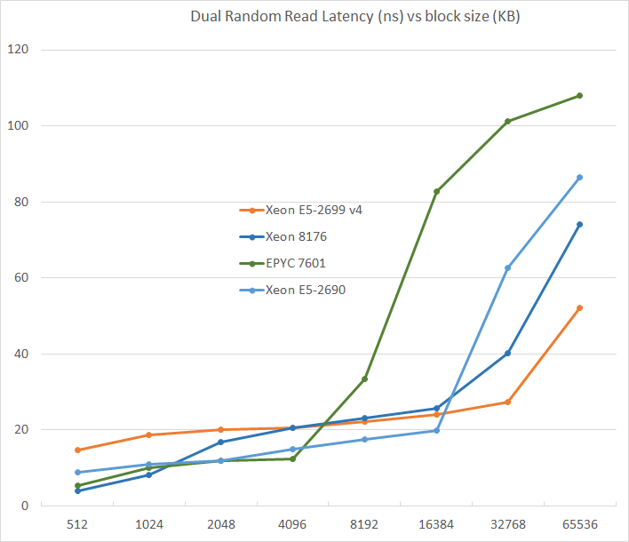
L3-cache sizes have increased steadily over the years. The Xeon E5 v1 had up to 20 MB, v3 came with 45 MB, and v4 "Broadwell EP" further increased this to 55 MB. But the fatter the cache, the higher the latency became. L3 latency doubled from Sandy Bridge-EP to Broadwell-EP. So it is no wonder that Skylake went for a larger L2-cache and a smaller but faster L3. The L2-cache offers 4 times lower latency at 512 KB.
AMD's unloaded latency is very competitive under 8 MB, and is a vast improvement over previous AMD server CPUs. Unfortunately, accessing more 8 MB incurs worse latency than a Broadwell core accessing DRAM. Due to the slow L3-cache access, AMD's DRAM access is also the slowest. The importance of unloaded DRAM latency should of course not be exaggerated: in most applications most of the loads are done in the caches. Still, it is bad news for applications with pointer chasing or other latency-sensitive operations.


219 Comments
View All Comments
psychobriggsy - Tuesday, July 11, 2017 - link
Indeed it is a ridiculous comment, and puts the earlier crying about the older Ubuntu and GCC into context - just an Intel Fanboy.In fact Intel's core architecture is older, and GCC has been tweaked a lot for it over the years - a slightly old GCC might not get the best out of Skylake, but it will get a lot. Zen is a new core, and GCC has only recently got optimisations for it.
EasyListening - Wednesday, July 12, 2017 - link
I thought he was joking, but I didn't find it funny. So dumb.... makes me sad.blublub - Tuesday, July 11, 2017 - link
I kinda miss Infinity Fabric on my Haswell CPU and it seems to only have on die - so why is that missing on Haswell wehen Ryzen is an exact copy?blublub - Tuesday, July 11, 2017 - link
Your actually sound similar to JuanRGA at SAKevin G - Wednesday, July 12, 2017 - link
@CajunArson The cache hierarchy is radically different between these designs as well as the port arrangement for dispatch. Scheduling on Ryzen is split between execution resources where as Intel favors a unified approach.bill.rookard - Tuesday, July 11, 2017 - link
Well, that is something that could be figured out if they (anandtech) had more time with the servers. Remember, they only had a week with the AMD system, and much like many of the games and such, optimizing is a matter of run test, measure, examine results, tweak settings, rinse and repeat. Considering one of the tests took 4 hours to run, having only a week to do this testing means much of the optimization is probably left out.They went with a 'generic' set of relative optimizations in the interest of time, and these are the (very interesting) results.
CoachAub - Wednesday, July 12, 2017 - link
Benchmarks just need to be run on as level as a field as possible. Intel has controlled the market so long, software leans their way. Who was optimizing for Opteron chips in 2016-17? ;)theeldest - Tuesday, July 11, 2017 - link
The compiler used isn't meant to be the the most optimized, but instead it's trying to be representative of actual customer workloads.Most customer applications in normal datacenters (not google, aws, azure, etc) are running binaries that are many years behind on optimizations.
So, yes, they can get better performance. But using those optimizations is not representative of the market they're trying to show numbers for.
CajunArson - Tuesday, July 11, 2017 - link
That might make a tiny bit of sense if most of the benchmarks run were real-world workloads and not C-Ray or POV-Ray.The most real-world benchmark in the whole setup was the database benchmark.
coder543 - Tuesday, July 11, 2017 - link
The one benchmark that favors Intel is the "most real-world"? Absolutely, I want AnandTech to do further testing, but your comments do not sound unbiased.