Sizing Up Servers: Intel's Skylake-SP Xeon versus AMD's EPYC 7000 - The Server CPU Battle of the Decade?
by Johan De Gelas & Ian Cutress on July 11, 2017 12:15 PM EST- Posted in
- CPUs
- AMD
- Intel
- Xeon
- Enterprise
- Skylake
- Zen
- Naples
- Skylake-SP
- EPYC
Memory Subsystem: Latency
The performance of modern CPUs depends heavily on the cache subsystem. And some applications depend heavily on the DRAM subsystem too. We used LMBench in an effort to try to measure cache and memory latency. The numbers we looked at were "Random load latency stride=16 Bytes".
| Mem Hierarchy |
AMD EPYC 7601 DDR4-2400 |
Intel Skylake-SP DDR4-2666 |
Intel Broadwell Xeon E5-2699v4 DDR4-2400 |
| L1 Cache cycles | 4 | 4 | 4 |
| L2 Cache cycles | 12 | 14-22 | 12-15 |
| L3 Cache 4-8 MB - cycles | 34-47 | 54-56 | 38-51 |
| 16-32 MB - ns | 89-95 ns | 25-27 ns (+/- 55 cycles?) |
27-42 ns (+/- 47 cycles) |
| Memory 384-512 MB - ns | 96-98 ns | 89-91 ns | 95 ns |
Previously, Ian has described the AMD Infinity Fabric that stitches the two CCXes together in one die and interconnects the 4 different "Zeppelin" dies in one MCM. The choice of using two CCXes in a single die is certainly not optimal for Naples. The local "inside the CCX" 8 MB L3-cache is accessed with very little latency. But once the core needs to access another L3-cache chunk – even on the same die – unloaded latency is pretty bad: it's only slightly better than the DRAM access latency. Accessing DRAM is on all modern CPUs a naturally high latency operation: signals have to travel from the memory controller over the memory bus, and the internal memory matrix of DDR4-2666 DRAM is only running at 333 MHz (hence the very high CAS latencies of DDR4). So it is surprising that accessing SRAM over an on-chip fabric requires so many cycles.
What does this mean to the end user? The 64 MB L3 on the spec sheet does not really exist. In fact even the 16 MB L3 on a single Zeppelin die consists of two 8 MB L3-caches. There is no cache that truly functions as single, unified L3-cache on the MCM; instead there are eight separate 8 MB L3-caches.
That will work out fine for applications that have a footprint that fits within a single 8 MB L3 slice, like virtual machines (JVM, Hypervisors based ones) and HPC/Big Data applications that work on separate chunks of data in parallel (for example, the "map" phase of "map/reduce"). However this kind of setup will definitely hurt the performance of applications that need "central" access to one big data pool, such as database applications and big data applications in the "Shuffle phase".
Memory Subsystem: TinyMemBench
To double check our latency measurements and get a deeper understanding of the respective architectures, we also use the open source TinyMemBench benchmark. The source was compiled for x86 with GCC 5.4 and the optimization level was set to "-O3". The measurement is described well by the manual of TinyMemBench:
Average time is measured for random memory accesses in the buffers of different sizes. The larger the buffer, the more significant the relative contributions of TLB, L1/L2 cache misses, and DRAM accesses become. All the numbers represent extra time, which needs to be added to L1 cache latency (4 cycles).
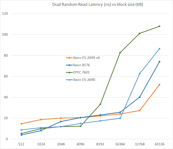
We tested with dual random read, as we wanted to see how the memory system coped with multiple read requests.
L3-cache sizes have increased steadily over the years. The Xeon E5 v1 had up to 20 MB, v3 came with 45 MB, and v4 "Broadwell EP" further increased this to 55 MB. But the fatter the cache, the higher the latency became. L3 latency doubled from Sandy Bridge-EP to Broadwell-EP. So it is no wonder that Skylake went for a larger L2-cache and a smaller but faster L3. The L2-cache offers 4 times lower latency at 512 KB.
AMD's unloaded latency is very competitive under 8 MB, and is a vast improvement over previous AMD server CPUs. Unfortunately, accessing more 8 MB incurs worse latency than a Broadwell core accessing DRAM. Due to the slow L3-cache access, AMD's DRAM access is also the slowest. The importance of unloaded DRAM latency should of course not be exaggerated: in most applications most of the loads are done in the caches. Still, it is bad news for applications with pointer chasing or other latency-sensitive operations.


219 Comments
View All Comments
oldlaptop - Thursday, July 13, 2017 - link
Why on earth is gcc -Ofast being used to mimic "real-world", non-"aggressively optimized"(!) conditions? This is in fact the *most* aggressive optimization setting available; it is very sensitive to the exact program being compiled at best, and generates bloated (low priority on code size) and/or buggy code at worst (possibly even harming performance if the generated code is so big as to harm cache coherency). Most real-world software will be built with -O2 or possibly -Os. I can't help but wonder why questions weren't asked when SPEC complained about this unwisely aggressive optimization setting...peevee - Thursday, July 13, 2017 - link
"added a second full-blown 512 bit AVX-512 unit. "Do you mean "added second 256 ALU, which in combination with the first one implements full 512-bit AVX-512 unit"?
peevee - Thursday, July 13, 2017 - link
"getting data from the right top node to the bottom left node – should demand around 13 cycles. And before you get too concerned with that number, keep in mind that it compares very favorably with any off die communication that has to happen between different dies in (AMD's) Multi Chip Module (MCM), with the Skylake-SP's latency being around one-tenth of EPYC's."1/10th? Asking data from L3 on the chip next to it will take 130 (or even 65 if they are talking about averages) cycles? Does not sound realistic, you can request data from RAM at similar latencies already.
AmericasCup - Friday, July 14, 2017 - link
'For enterprises with a small infrastructure crew and server hardware on premise, spending time on hardware tuning is not an option most of the time.'Conversely, our small crew shop has been tuning AMD (selected for scalar floating point operations performance) for years. The experience and familiarity makes switching less attractive.
Also, you did all this in one week for AMD and two weeks for Intel? Did you ever sleep? KUDOS!
JohanAnandtech - Friday, July 21, 2017 - link
Thanks for appreciating the effort. Luckily, I got some help from Ian on Tuesday. :-)AntonErtl - Friday, July 14, 2017 - link
According to http://www.anandtech.com/show/10158/the-intel-xeon... if you execute just one AVX256 instruction on one core, this slows down the clocks of all E5v4 cores on the same socket for at least 1ms. Somewhere I read that newer Xeons only slow down the core that executes the AVX256 instruction. I expect that it works the same way for AVX512, and yes, this means that if you don't have a load with a heavy proportion of SIMD instructions, you are better off with AVX128 or SSE. The AMD variant of having only 128-bit FPUs and no clock slowdown looks better balanced to me. It might not win Linpack benchmark competitions, but for that one uses GPUs anyway these days.wagoo - Sunday, July 16, 2017 - link
Typo on the CLOSING THOUGHTS page: "dual Silver Xeon solutions" (dual socket)Great read though, thanks! Can finally replace my dual socket shanghai opteron home server soon :)
Chaser - Sunday, July 16, 2017 - link
AMD's CPU future is looking very promising!bongey - Tuesday, July 18, 2017 - link
EPYC power consumption is just wrong. Somehow you are 50W over what everyone else is getting at idle. https://www.servethehome.com/amd-epyc-7601-dual-so...Nenad - Thursday, July 20, 2017 - link
Interesting SPECint2006 results:- Intel in their slide #9 claims that Intel 8160 is 2% faster than EPYC 7601
- Anandtech in article tests that EPYC 7601 is 42% faster than Intel 8176
Those two are quite different, even if we ignore that 8176 should be faster than 8160. In other words, those Intel test results look very suspicious.