Semiconductors
Taiwan Semiconductor Manufacturing Co. this week said its revenue for the second quarter 2024 reached $20.82 billion, making it the company's best quarter (at least in dollars) to date. TSMC's high-performance computing (HPC) platform revenue share exceeded 52% for the first time in many years due to demand for AI processors and rebound of the PC market. TSMC earned $20.82 billion USD in revenue for the second quarter of 2024, a 32.8% year-over-year increase and a 10.3% increase from the previous quarter. Perhaps more remarkable, $20.82 billion is a higher result than the company posted Q3 2022 ($20.23 billion), the foundry's best quarter to date. Otherwise, in terms of profitability, TSMC booked $7.59 billion in net income for the quarter, for a gross margin of...
TSMC Preps 6x Reticle Size Super Carrier Interposer for Extreme SiP Processors
As part of their efforts to push the boundaries on the largest manufacturable chip sizes, Taiwan Semiconductor Manufacturing Co. is working on its new Chip-On-Wafer-On-Substrate-L (CoWoS-L) packaging technology that...
2 by Anton Shilov on 5/26/2023
TSMC Details N4X Process for HPC: Extreme Performance at Minimum Leakage
At its 2023 Technology Symposium TSMC revealed some additional details about its upcoming N4X technology that is designed specifically for high-performance computing (HPC) applications. This node promises to enable...
5 by Anton Shilov on 5/26/2023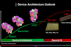
TSMC: We Have Working CFET Transistors in the Lab, But They Are Generations Away
Offering an update on its work with complementary field-effect transistors (CFETs) as part of the company's European Technology Symposium 2023, TSMC has revealed that it has working CFETs within...
3 by Anton Shilov on 5/25/2023
Samsung to Unveil Refined 3nm and Performance-Enhanced 4nm Nodes at VLSI Symposium
Samsung Foundry is set to detail its second generation 3 nm-class fabrication technology as well as its performance-enhanced 4 nm-class manufacturing process at the upcoming upcoming 2023 Symposium on...
3 by Anton Shilov on 5/10/2023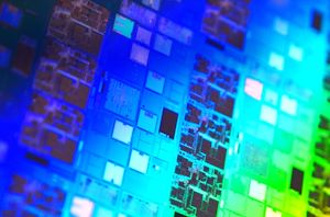
Samsung Foundry Vows to Surpass TSMC Within Five Years
The head of Samsung's semiconductor unit acknowledged last week that the company's current mass production, leading-edge process technologies are a couple of years behind TSMC's most advanced production nodes...
18 by Anton Shilov on 5/8/2023
TSMC Announces Early Access Nodes for Next-Gen Car Chips: N4AE and N3AE
As the final set of announcements from this week's North American Technology Symposium, TSMC closed out their fab roadmap updates with some fresh news on their automotive-centric processes. For...
10 by Anton Shilov on 4/28/2023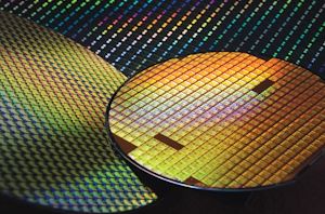
TSMC Details 3nm Evolution: N3E On Schedule, N3P and N3X To Deliver 5% Performance Gains
Alongside some new announcements for their 2nm process node plans, TSMC has also released a progress and roadmap update for their N3 family process technologies at today's 2023 North...
13 by Anton Shilov on 4/26/2023
TSMC Outlines 2nm Plans: N2P Brings Backside Power Delivery in 2026, N2X Added To Roadmap
At its 2023 North American Technology Symposium today, TSMC has disclosed additional details about its plans for its forthcoming N2 2nm-class production nodes in 2025 – 2026 and beyond...
38 by Anton Shilov on 4/26/2023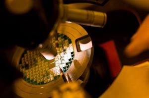
GlobalFoundries Sues IBM Over Sharing Leading-Edge Chip IP with Intel, Rapidus
The relationship between GlobalFoundries and IBM has been rocky in recent years. Among other things, Big Blue has previously sued GF, seeking damages for abruptly stopping the development of...
10 by Anton Shilov on 4/20/2023
Synopsys Intros AI-Powered EDA Suite to Accelerate Chip Design and Cut Costs
Synopsys has introduced the industry's first full-stack AI-powered suite of electronic design automation tools that covers all stages of chip design, from architecture to design and implementation to manufacturing...
12 by Anton Shilov on 3/30/2023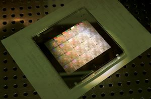
NVIDIA's cuLitho to Speed Up Computational Lithography for 2nm and Beyond
Production of chips using leading-edge process technologies requires more compute power than ever. To address requirements of 2nm nodes and beyond, NVIDIA is rolling out its cuLitho software library...
31 by Anton Shilov on 3/27/2023
Gordon Moore, Intel's Co-Founder and Tech Industry Visionary, Passes Away At 94
Intel and the Gordon and Betty Moore Foundation have announced this evening that Gordon Moore, Intel’s famous co-founder and grandfather to much of the modern chip industry, has passed...
20 by Ryan Smith on 3/24/2023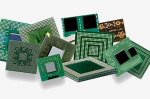
Out With Organic, In With Glass? DNP Unveils Glass Core Substrate Tech For Chips
As the chip industry develops more sophisticated processors with higher heat dissipation requirements, some firms have moved on to chiplet-based designs. This not-so-gradual shift has resulted in chip packaging...
17 by Anton Shilov on 3/23/2023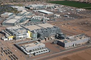
Inflation Drives Up Fab Costs for Intel and Samsung by Billions of Dollars
To address future demand for semiconductors amid severe chip shortages of 2020 – 2022, all leading chipmakers announced plans to build new fabs and even disclosed their estimated costs...
15 by Anton Shilov on 3/16/2023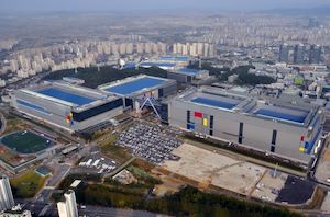
Samsung Seeks to Make South Korea No. 1 Chipmaker with $230B Investment Over 20 Years
Samsung on Wednesday unveiled their plan to invest $230 billion over the next 20 years in a new semiconductor production mega cluster in South Korea. The country's government believes...
22 by Anton Shilov on 3/15/2023
TSMC's 3nm Journey: Slow Ramp, Huge Investments, Big Future
Last week, TSMC issued their Q4 and full-year 2022 earnings reports for the company. Besides confirming that TSMC was closing out a very busy, very profitable year for the...
30 by Anton Shilov on 1/17/2023
TSMC Unveils Major U.S. Fab Expansion Plans: 3nm and $40 Billion by 2026
TSMC this week held its Arizona fab 'first tool-in' ceremony, where alongside celebrating its first US fab, the company also announced major expansion plans for the production facility. The...
17 by Anton Shilov on 12/7/2022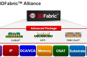
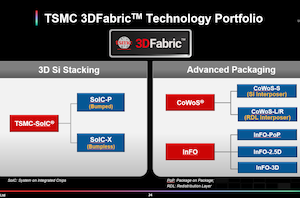
TSMC Forms 3DFabric Alliance to Accelerate Development of 2.5D & 3D Chiplet Products
Currently the majority of high-end processors are monolithic, but design methodologies are slowly but surely shifting to multi-chiplet modules as leading-edge fabrication technologies get more expensive to use. In...
9 by Anton Shilov on 10/27/2022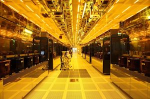
Micron Announces 20-Year Plan To Build $100 Billion U.S. Fab Complex
Now that the U.S. government has finally settled the matter of whether it would be providing subsidies to entice chip fabs to setup shop within the U.S., those fabs...
48 by Anton Shilov on 10/10/2022
Samsung Foundry Outlines Roadmap Through 2027: 1.4 nm Node, 3x More Capacity
Samsung outlined its foundry business roadmap for the next five years at its Foundry Forum event last week. The company plans to introduce its next generation fabrication technologies in...
14 by Anton Shilov on 10/10/2022


