Hot Chips 2018: The Google Pixel Visual Core Live Blog (10am PT, 5pm UTC)
by Ian Cutress on August 20, 2018 12:45 PM EST12:46PM EDT - Hot Chips has started! One of the first talks today is from Google, detailing the Pixel Visual Core processor found in the latest Pixel smartphones. The talk is called 'The Pixel Visual Core: Google’s Fully Programmable Image, Vision and AI Processor for Mobile Devices'
12:47PM EDT - If you're not deep into the NVIDIA Live Blog, then this talk should be interesting

12:49PM EDT - at least half a dozen live blogs today on different topics
12:49PM EDT - We'll go over some of the talks in proper analysis pieces in due course, with all the slides
12:50PM EDT - These talks usually go quite quick, we're just finishing up the previous talk
12:56PM EDT - OK here we go. Speaker is Jason Redgrave
12:56PM EDT - Four years of development on the PVC
12:57PM EDT - Motivation is to make pictures look better
12:57PM EDT - The way users imagine them
12:57PM EDT - Computational photography
12:58PM EDT - Hard to bake algorithms into the hardware early because they change so often
12:58PM EDT - Need to match expectations without being late
12:59PM EDT - Need something programmable
12:59PM EDT - CPU and GPU consume too much power
12:59PM EDT - Compute needed vs energy vs op
12:59PM EDT - Don't get efficiency with current programmable parts
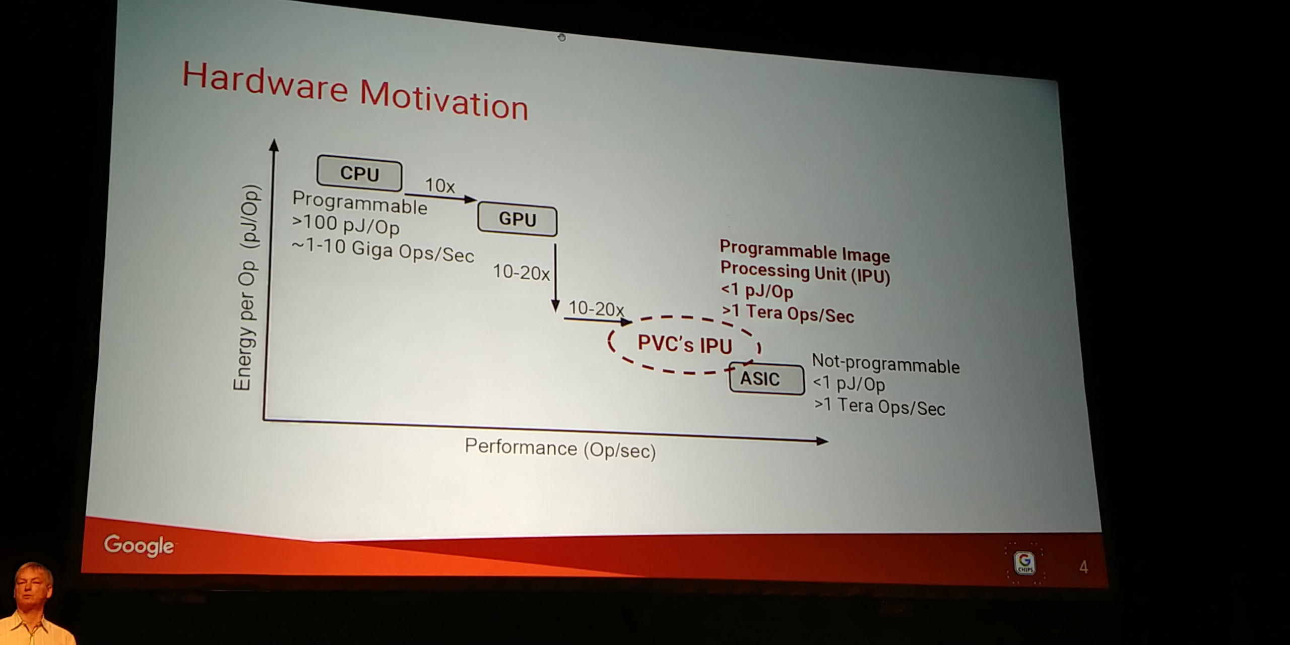
01:00PM EDT - GPUs don't take advantage of image processing patterns compared to custom silicon
01:00PM EDT - Moving into a customized domain, just before a dedicated ASIC
01:00PM EDT - Set the tone from a software PoV
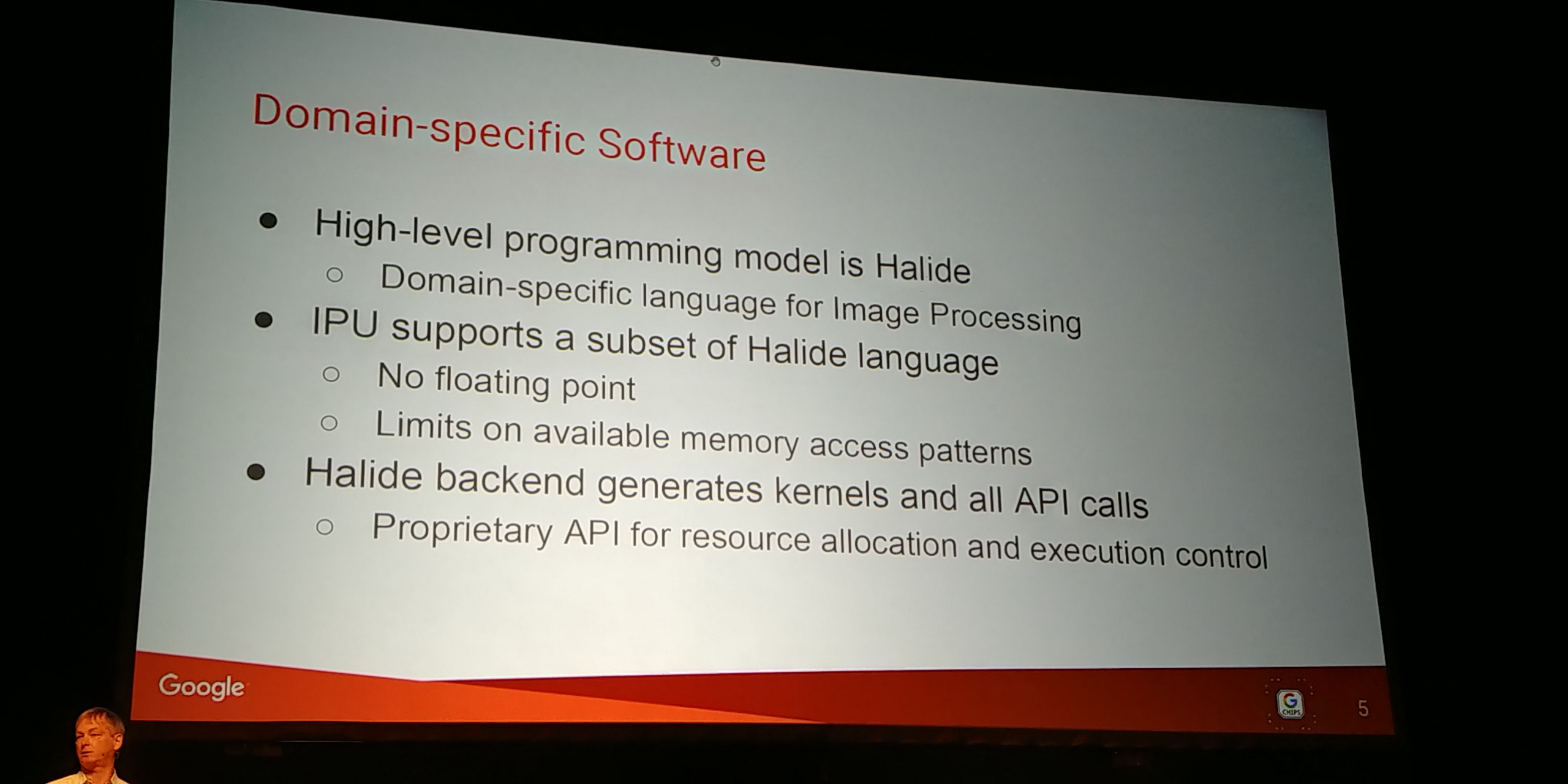
01:01PM EDT - HDR was already built in Halide language
01:01PM EDT - PVC supports a subset of Halide
01:01PM EDT - PVC doesn't support floating point
01:01PM EDT - Limits on memory access patterns
01:02PM EDT - In future, looking to support FP to reduce friction on moving applications to processor
01:02PM EDT - Built a Halide back-end which works with custom formats needed
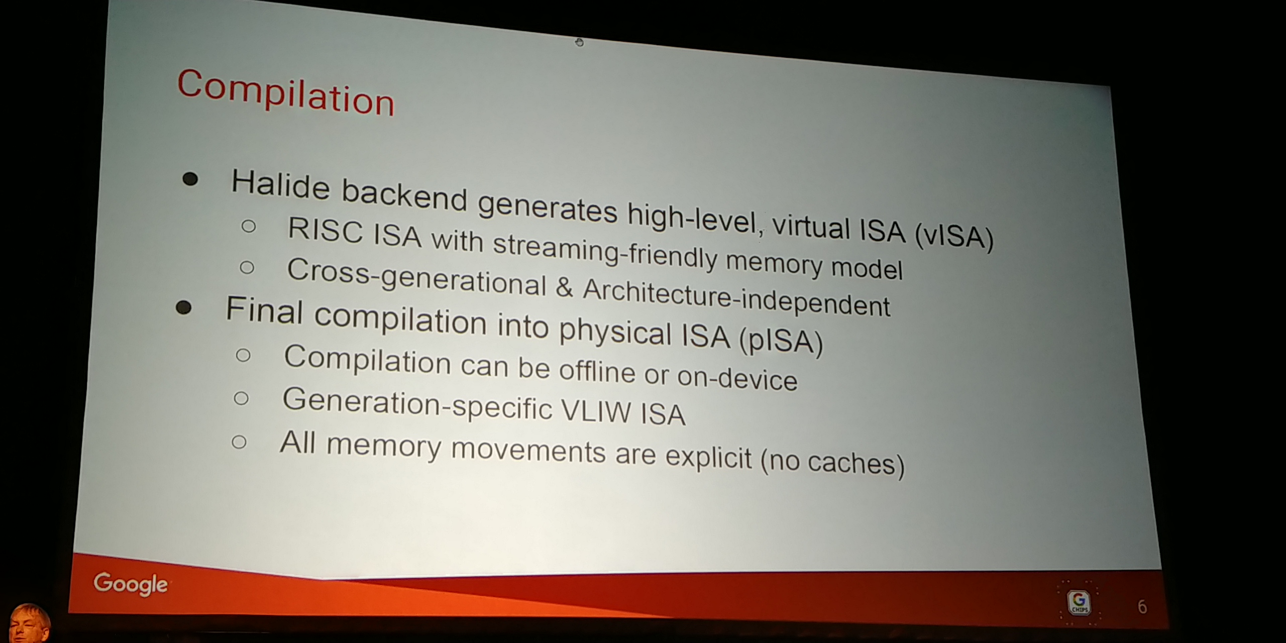
01:02PM EDT - Don't make hardware block that is limited by ISA and process
01:03PM EDT - Reducing hoops from gen to gen
01:03PM EDT - High level virtual ISA used instead
01:03PM EDT - Compile to that high-level ISA
01:03PM EDT - Have translation layer to current version of hardware
01:03PM EDT - Can do in a JIT mode if needed
01:03PM EDT - Currently a VLIW architecture
01:03PM EDT - Fitting memory movements at time of compute
01:03PM EDT - Next to no caches
01:04PM EDT - Primary mode is knowing memory location at time of compile

01:04PM EDT - Most ASICs do stencil operations
01:04PM EDT - The value of a pixel is a function of the pixle and pixels around it
01:05PM EDT - Compute is over a pixel range to calculate new pixel
01:05PM EDT - Requires a lot of data
01:05PM EDT - These are line buffers
01:05PM EDT - from a hardware PoV, need stencil processors
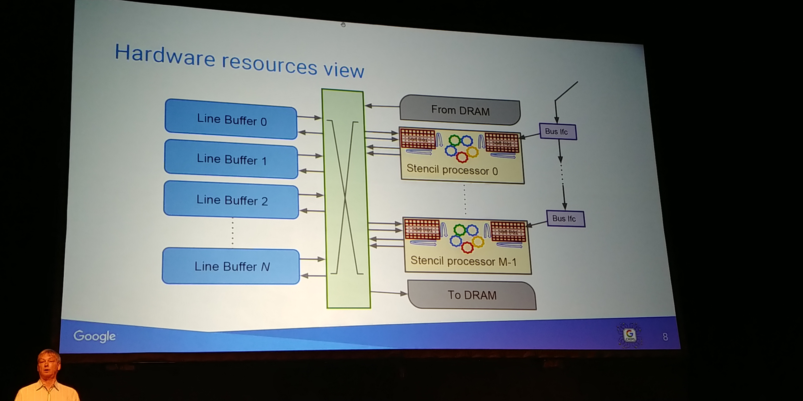
01:06PM EDT - Do more of the co-pressing and save the SoC
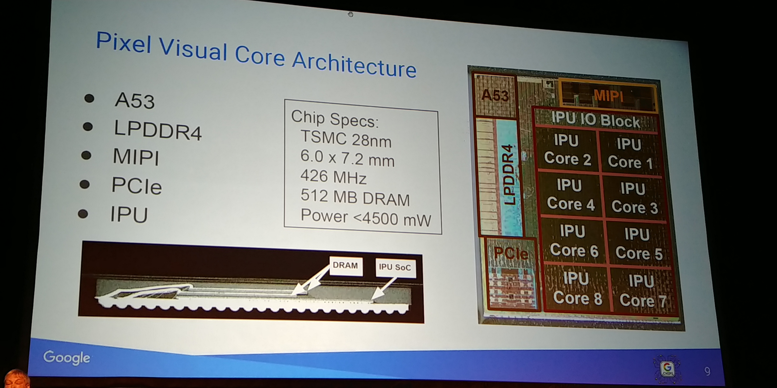
01:06PM EDT - PVC is a full SoC
01:06PM EDT - A53, LPDDR4, PCIe
01:07PM EDT - IPU core has an IO block
01:07PM EDT - dealing with MIPI streams
01:07PM EDT - Currently an 8-core
01:07PM EDT - Each IPU core is a stencil processor and a line buffer pool
01:07PM EDT - TSMC 28nm
01:07PM EDT - Built as SiP
01:07PM EDT - DRAM stacked on top of die
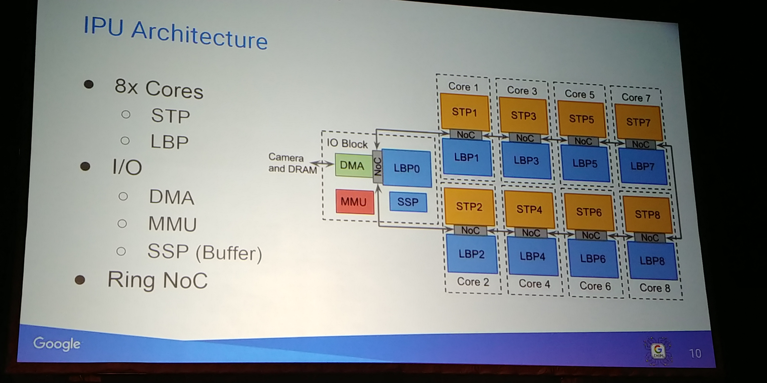
01:08PM EDT - SIMD array of processsors
01:08PM EDT - (this is the line buffer pool)
01:08PM EDT - Connect out to AXI fabric
01:08PM EDT - Ring NoC
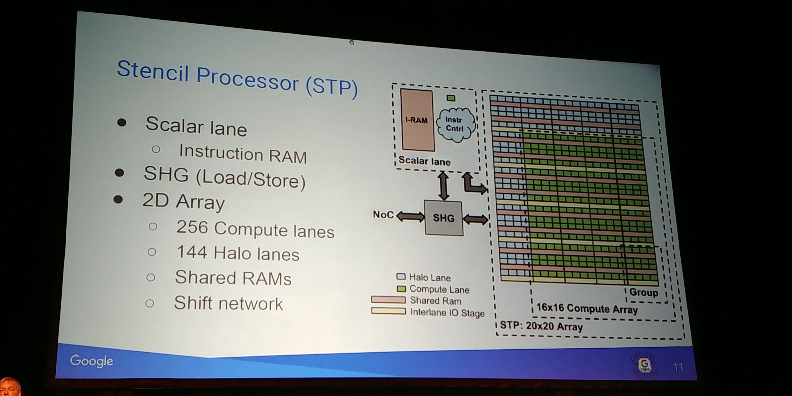
01:09PM EDT - Build an array for pixels for stencil processor (STP)
01:09PM EDT - Block level looks like other SIMD procs
01:09PM EDT - VLIW in vector lanes
01:09PM EDT - different instructions for load/store in vector
01:09PM EDT - Sheet memory accesses
01:09PM EDT - support different sizes
01:10PM EDT - Halo lanes as well
01:10PM EDT - 20x20 array can support 16x16 sheets with halo regions
01:10PM EDT - Dont have compute resources, just memory resources
01:10PM EDT - Share RAMs across 2x8 ALU arrays
01:10PM EDT - Purely for PPA considerations
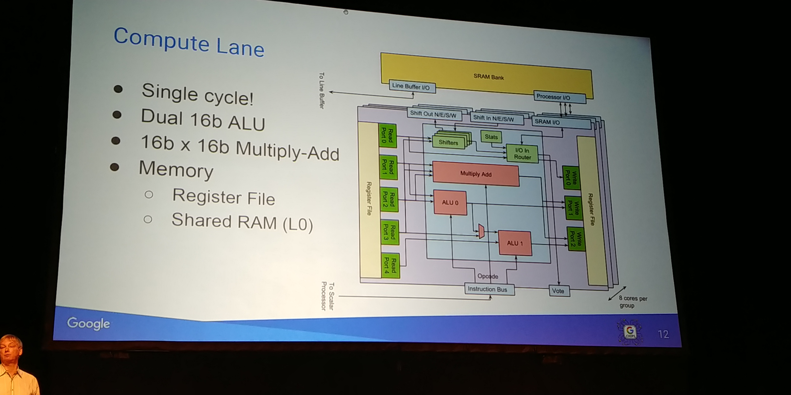
01:11PM EDT - Built as a single cycle multiple-accumulate
01:11PM EDT - Dual 16b ALU per cycle
01:11PM EDT - Support for fixed point
01:11PM EDT - Memory access is simultaneous
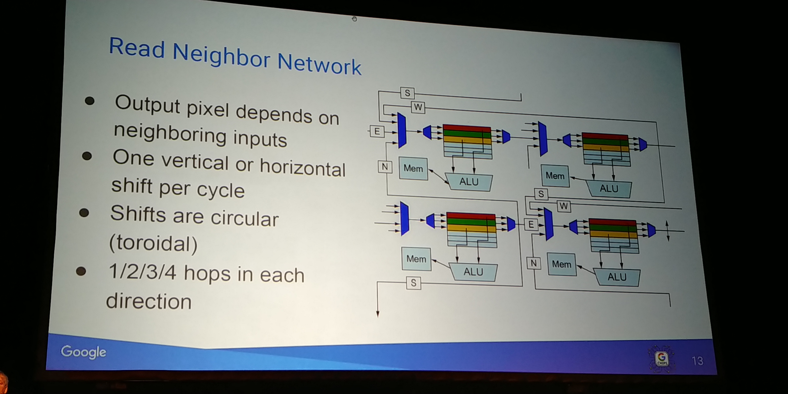
01:12PM EDT - Shift network / read neighbor network
01:12PM EDT - used to save engine
01:12PM EDT - energy
01:12PM EDT - Have to have a way to get data between lanes, and data back to register vector file
01:13PM EDT - Also want to keep it simple - 10-entry register per compute
01:13PM EDT - Data needed is often in a neighbor
01:13PM EDT - can access from neighboring lanes (up to 4 hops) in a single cycle
01:14PM EDT - VLIW can do it parallel with compute
01:14PM EDT - This contrinutes a lot to energy efficiency

01:14PM EDT - Also Line Buffers
01:14PM EDT - Pool is shared storage with pointers into that storage - implements 2D FIFOs
01:15PM EDT - Buffer a portion of the image as it is streamed through it related to the array of pixel processors
01:15PM EDT - Maintain sync over processor
01:15PM EDT - Sync is based by hardware pointers that are updated by software
01:16PM EDT - Includes the ability to query the status of the line buffers
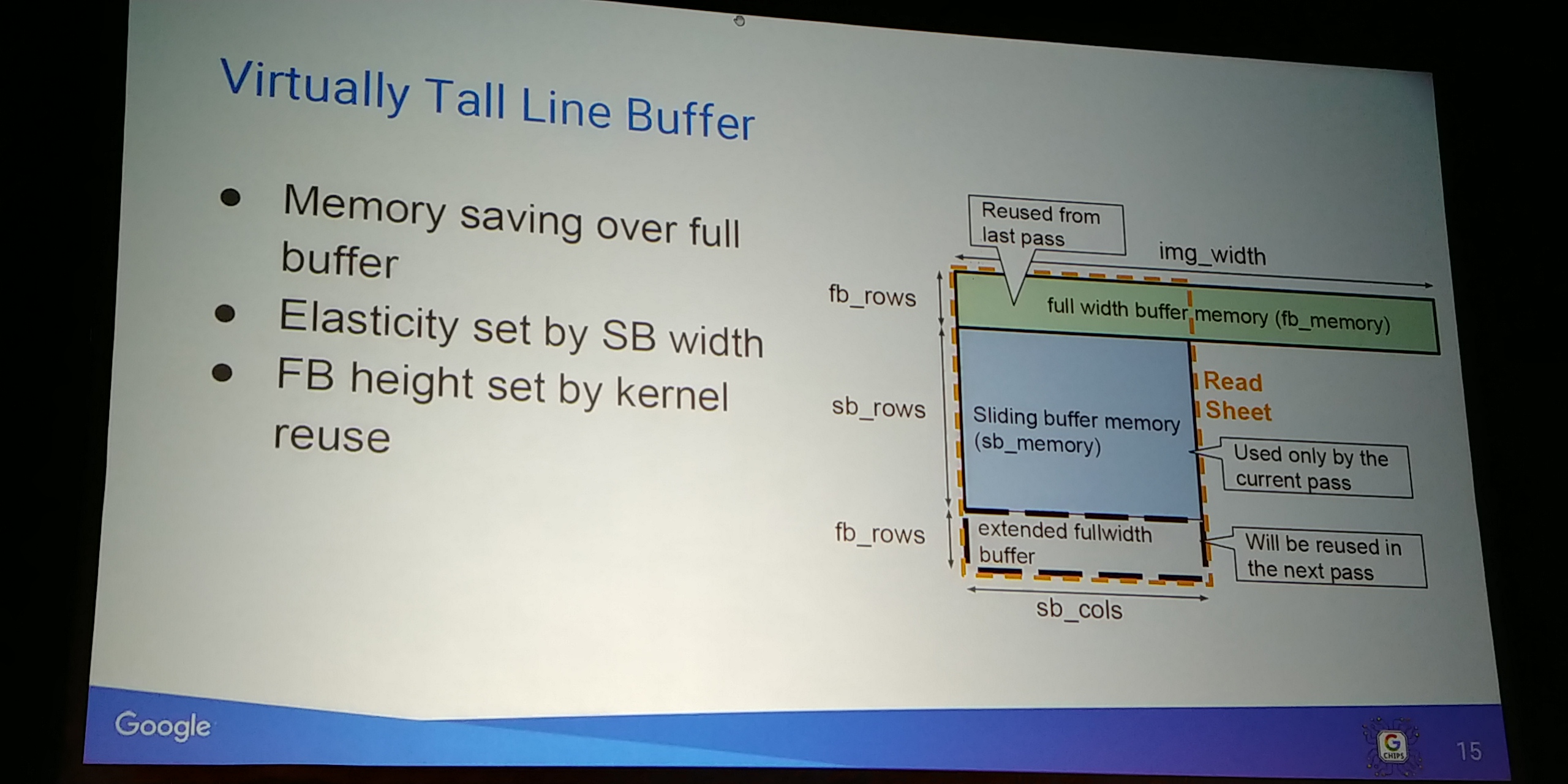
01:17PM EDT - Most of the time the data needed to retain across a horizontal pass is less than the size of the number of rows being processed
01:17PM EDT - Sub-divide the memory and buffer only the rows needed to save area and power
01:18PM EDT - Especially with less memory overall
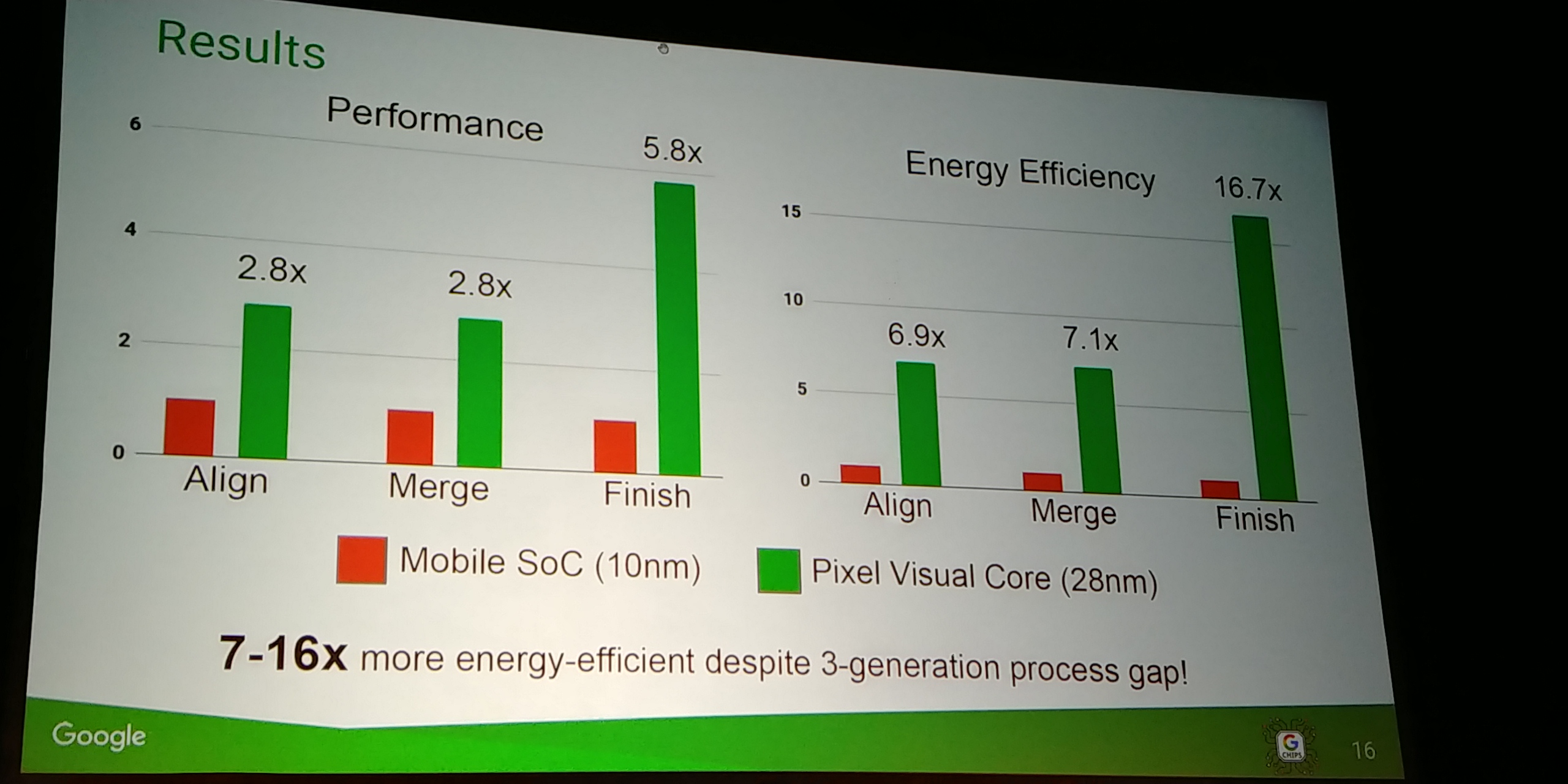
01:18PM EDT - Results on Pixel 2
01:18PM EDT - HDR2+ data
01:18PM EDT - 28nm PVC vs 10nm SoC
01:19PM EDT - Normalised for perf and energy efficiency
01:19PM EDT - Over 50 people in the PVC team
01:20PM EDT - Q&A time
01:21PM EDT - Q: Dev process was long, didn't aim to design for specific algorithms. Find any surprises when hardware was done?
01:21PM EDT - A: We worried about the friction for use. It's programmable and you need a tool chain. Often more work than the hardware! Personally we should have worried about that friction more.
01:22PM EDT - Q: In early project definition to support Halide. How did you decide what to accelerate?
01:23PM EDT - A: We knew we wanted to accel HDR+. We had the team to map algorithms for normal visual processing. We say how well did they map, did we miss something, is there some aspect we need to do better
01:23PM EDT - Q: Does the arch adapt from classic algorithms to NN algorithms?
01:24PM EDT - A: HDR+ covers a wide range of algorithms - axial discrete FFTs are a part of that. It works quite well for that - as long as you don't drift that need divergent memory accesses, the cores are flexible
01:24PM EDT - Q: Perf numbers compared with CPU/GPU, or with DSP?
01:24PM EDT - A: Comparison against production software. Not sure how much was running on DSP
01:25PM EDT - Q: Any consider going beyond phones with the hardware?
01:25PM EDT - A: Can't speculate about the future.
01:26PM EDT - That's a wrap! Next talk in an hour


14 Comments
View All Comments
NeoteriX - Monday, August 20, 2018 - link
I wish the consumer-facing story around the Pixel Visual Core was much clearer. I remember shortly after launch when it was announced that the phone shipped with the PVC, that the story went back and forth as to whether it was being used at all or was even needed, or in what cases it would be used.shadowx360 - Monday, August 20, 2018 - link
None of that is unclear....a quick Google would have told you that they enabled it shortly after launch with an update, and now third party apps like Snapchat use the PVC so snaps now look slightly less potato.NeoteriX - Monday, August 20, 2018 - link
https://www.theverge.com/circuitbreaker/2018/2/8/1...Are you sure about that? This sources suggests the PVC only works for 3rd party apps... which means for whatever reason, the regular camera app is not benefitting from the optimized power/performance of the PVC.
SharpEars - Monday, August 20, 2018 - link
28nm? Seriously? Not interested at all...shadowx360 - Monday, August 20, 2018 - link
The fact that it was built in 28nm takes nothing from those results in the final slide.tipoo - Tuesday, August 21, 2018 - link
That just makes a 16x gain more impressive.Maybe 28nm was cheaper, if it's that much faster and fast enough that they didn't see a new nodes benefits, why does that matter to you?
tipoo - Monday, August 20, 2018 - link
Did they turn this on in the Pixel 2 yet, and what kind of difference did it make?They launched without using the unit, and the camera was already impressive, perhaps the best in a phone
shadowx360 - Monday, August 20, 2018 - link
They turned it on with the first update for Android Oreo last year. Mostly just speeds up the processing with lowered battery usage for the stock camera, but real value was allowing third party apps like notoriously bad Snapchat to have decent looking shots.PeachNCream - Monday, August 20, 2018 - link
I know improving photo quality is an important feature, but that's a lot of dedicated hardware and research which will invariably come at a cost passed along to the consumer that makes getting high-end stuff more expensive without adding something that a decent number of us that just want okay looking pics of our cats will find very useful.shadowx360 - Monday, August 20, 2018 - link
Flagships sell for close to $1000 regardless. Now would you rather they spend some R&D money into the camera or just give you "okay looking pics" and still charge you the same price? If that's what you need, go buy a mid-range device and save your money.