The Samsung Exynos 7420 Deep Dive - Inside A Modern 14nm SoC
by Andrei Frumusanu on June 29, 2015 6:00 AM ESTGPU Performance & Power
Continuing on to the GPU side of the Exynos 7420, we’re again revisiting ARM’s Mali T760. We’ve extensively covered ARM’s Midgard series and Samsung’s implementation in our in-depth architectural article as well as the Note 4 Exynos review. The Exynos 7420 isn’t too different to the 5433 on the GPU side other than having 2 additional shader cores and being able to take advantage of LPDDR4 memory. While we’re pretty sure of the impact the two added shader cores will have, the new memory technology and increased bandwidth it brings is still an unknown until we take a deep look at how performance scales with the faster memory.
First we take a look at peak power consumption of the 7420 and how it compared to other SoCs we currently have numbers on. For this we measure power during GFXBench’s T-Rex and Manhattan 3.0 tests in off-screen mode.
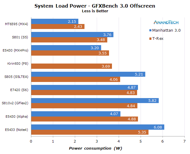
The Galaxy S6 and Exynos 7420 use up to 4.85W of load power. Again, load power here means the figures have the device’s idle and the screen power consumption subtracted to give a better view of the active SoC power instead of the device as a whole.
The 14nm manufacturing process looks to have allowed Samsung to increase performance while still improving power over the 5433’s T760MP6 which runs at slightly lower clocks. We previously investigated Samsung’s curious DVFS technique for ARM’s Midgard architecture and it seems the Exynos 7420 does a much better job at balancing out power when the GPU handles ALU-heavy loads. As a reminder, Samsung chooses to clock the GPUs higher whenever a given task puts a more ALU-centric load on the shader cores. In the case of the Exynos 7420 the GPU runs up to 772MHz in this mode while loads which stress the texture- and load/store-units cap the maximum frequency at 700MHz. On the Exynos 5433 for example these limits were set at respectively 700 and 600MHz, so the 7420 has a comparatively smaller boost. The voltage difference between the two top states is also not as high as on the 5433, and both factors combined result that the GPU power difference between high-arithmetic and normal loads is minimal.
I finally had the opportunity to measure Qualcomm’s Adreno GPU's in the form of the Snapdragon 801, 805 and 810 in the S5, S5 LTE-A and G Flex2, and it showed some revealing numbers that I hadn’t expected. Firstly, it’s now very clear how the Adreno 420 was able to outperform the Mali T760MP6 between the two Note 4 variants as the power and efficiency difference on the T-Rex test is significant. What is interesting to see though is the Adreno 4xx's much higher power draw on ALU heavy loads such as the Manhattan test. While the Midgard architecture seems to allow the GPU a power advantage in arithmetic loads, the Adreno 4xx sees the complete opposite as its power draw increases dramatically.
To have a better picture of overall efficiency between the various architectures, I laid out both the performance and power numbers in a table overview:
| T-Rex Offscreen Power Efficiency (System Load Power) |
||||||
| Mfc. Process |
FPS | Avg. Power | Perf/W Efficiency |
|||
| Exynos 7420 (S6) | 14LPE | 56.3 | 4.82W | 11.63 fps/W | ||
| Snapdragon 805 (S5LTEA) | 28HPM | 40.7 | 4.06W | 10.02 fps/W | ||
| MT6595 (MX4) | 28HPM | 23.3 | 2.42W | 9.55 fps/W | ||
| Snapdragon 810 (G Flex2) | 20SoC | 45.5 | 4.84W | 9.39 fps/W | ||
| Exynos 5430 (MX4Pro) | 20LPE | 28.7 | 3.55W | 8.08 fps/W | ||
| Snapdragon 801 (S5) | 28HPM | 26.9 | 3.47W | 7.77 fps/W | ||
| Exynos 5433 (Note 4) | 20LPE | 37.3 | 5.35W | 6.97 fps/W | ||
| Exynos 5430 (Alpha) | 20LPE | 31.3 | 4.88W | 6.41 fps/W | ||
| Kirin 930 (P8 Estimated) | 28HPM | 17.0 | 3.69W | 4.60 fps/W | ||
While the Exynos 7420 draws a high amount of power at 4.82W, it also is able to post by far the best performance and thus ends up at the top of the efficiency table. While Qualcomm’s S805 has a full two process node disadvantage over the 7420, it is still able to just trail it in terms of power efficiency in the T-Rex test. The Adreno 430 of the Snapdragon 810 manages trail behind the Snapdragon 805 in efficiency even though it's on a better process node.
Things get shuffled around a bit in the more demanding and arithmetic heavy Manhattan test:
| Manhattan 3.0 Offscreen Power Efficiency (System Load Power) |
||||||
| Mfc. Process |
FPS | Avg. Power | Perf/W Efficiency |
|||
| Exynos 7420 (S6) | 14LPE | 24.8 | 4.87W | 5.08 fps/W | ||
| Exynos 5430 (MX4Pro) | 20LPE | 12.3 | 3.20W | 3.84 fps/W | ||
| MT6595 (MX4) | 28HPM | 8.1 | 2.15W | 3.76 fps/W | ||
| Snapdragon 805 (S5LTEA) | 28HPM | 18.2 | 5.20W | 3.66 fps/W | ||
| Snapdragon 810 (G Flex2) | 20SoC | 22.2 | 5.82W | 3.34 fps/W | ||
| Snapdragon 801 (S5) | 28HPM | 11.9 | 3.75W | 3.17 fps/W | ||
| Exynos 5430 (Alpha) | 20LPE | 12.7 | 4.07W | 3.11 fps/W | ||
| Exynos 5433 (Note 4) | 20LPE | 17.5 | 6.08W | 2.87 fps/W | ||
The Exynos 7420 remains at the top as the most efficient chipset, but this time it managed to do this by a considerable margin as Qualcomm’s Adreno 4xx's fall off behind other SoCs. We will be revisiting the Snapdragon 810 in more detail in a separate future article but for now the GFXBench results show that the chipset has actually lost efficiency over the Snapdragon 805 in both GFXBench tests even though it moved to a newer 20SoC TSMC manufacturing process.
It's clear that Samsung currently holds the efficiency crown due to the 14nm process, therefor it's hard to judge the efficiencies of the GPU architectures as we're not on an even playing field. It seems we’ll only be able to have a clear apples-to-apples architectural comparison once Qualcomm releases the Snapdragon 820 on a FinFET process.
People may have noticed I started including GPU numbers from MediaTek’s MT6595 with the review of the P8 and post them here as well. Even though absolute performance of the SoC is inferior, it’s the power consumption value which stands out as unusual. The chipset doesn’t exceed 2.4W at its top performance level, and this is quite telling of the design decisions between the different semiconductor vendors.
Over >3-4W, basically all SoCs tested will never be able to maintain their top frequency for any amount of reasonable and usable amount of time. We also see this in the Exynos 7420 as even with the new manufacturing process and its large efficiency gains it’s not able to maintain more than the 350-420MHz states. Joshua had written about his experience with the thermal throttling mechanism in our initial review of the Galaxy S6, and it showed a very sinusoidal performance curve as the thermal management couldn’t decide which frequency state to maintain for prolonged periods of time. I investigated this a bit and discovered that the throttling levels on the default driver were very steep and also weren’t gradual as one would expect. The stock driver has 4 throttling temperature levels and frequency caps configured at 544, 350, 266 and again 266MHz. This was odd to have two temperature thresholds at the same frequency as it doesn’t really makes for any practical use. I changed the throttling levels to 544, 420, 350 and 266MHz to allow for a more gradual degradation and also increased the power coefficient values on the IPA thermal management driver to values that seem more representative of the real-world measurements.
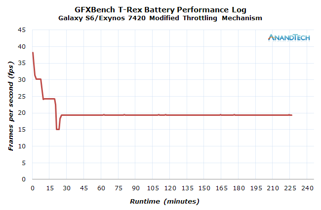
The end result is that instead of having performance behave very haphazardly during the duration of the run, we’re now able to achieve a consistent performance level once the temperature of the device settles in after 25 minutes. The rather shocking discovery is that this change was also able to increase battery performance by 33% as the S6 now lasted 3.8h instead of 2.8h on the stock settings. This change in runtime is due to the higher performance states having less efficiency than the lower states as we’re subject to linear power scaling on frequency and quadratic scaling of operating voltage.

We can see this in the load power measured at all of the GPU’s frequency states (The 772MHz state is missing due to T-Rex not scaling to that frequency). We see the 420MHz state use half the power of the 700MHz state even though it’s only 40% slower.
The mobile industry seems to have fallen into the bad habit of endlessly trying to one-up the competition in performance benchmarks that we have started to totally disregard total power and power efficiency. Other than MX4 with MediaTek’s MT6595 SoC (And seemingly Apple’s recent A-series SoCs) none of the recent flagship SoCs seem to employ a sensible GPU configuration that is able to actually maintain its maximum performance states. This unfortunately comes at the cost of the user experience - as demonstrated in the modified thermal throttling behavior; actually aiming for highest performance although it’s physically not possible due to thermal constraints will lead to inconsistent performance and reduced battery life.
In the case of the Galaxy S6 the GPU is not able to maintain the maximum frequency for more than 2 minutes and throttles to half the performance after about 20 minutes. Unless there are users whose gaming experiences are limited to 5-10 minute sessions it’s very hard to see a reasonable explanation for such settings. It would have been much better if vendors would cap the maximum possible frequency to the actual sustainable performance levels of their devices; in the case of the Galaxy S6 this seems to be the 420 or 350MHz states. It’s understandable that measuring efficiency is much harder than measuring pure synthetic performance, and as long as the industry and media don’t change their evaluation methodology for mobile devices this will unfortunately continue to be a large problem.
Similar to the CPU measurements, I was curious to see the impact of undervolting on 3D power consumption. To do this I again made an interface to be able to control the GPU’s power management driver and change the voltage tables on the fly, resulting in the following values for GFXBench T-Rex:
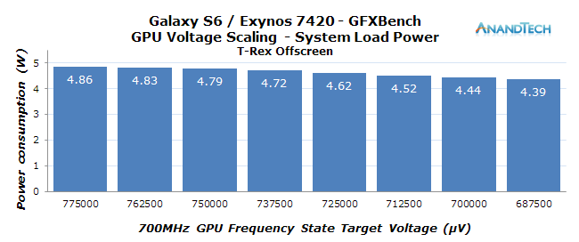
Given a cold device the benchmark will cause the GPU to remain at its maximum frequency state as long as it’s not V-sync limited. Given that T-Rex still doesn’t reach that point and that this is an off-screen test without V-sync, it’s something which we needn't have to worry about. I gradually reduced down voltage in 12.5mV steps until the device crashed and wasn’t able to complete the test run anymore. Overall, it seems the power gains are more limited than what we were able to achieve on the A57 cores. This is most likely due to the fact that the power numbers we’re seeing here are not only purely result of the GPU but also some CPU, interconnect, and most importantly memory controller and DRAM power.
LPDDR4 Performance & Power
LPDDR4 promises to bring some large power and performance advantages over LPDDR3. The performance advantages are clear as the new memory technology is able to double up on the available bandwidth to the whole of the SoC, increasing from 13.2GB/s for 825MHz LPDDR3 up to 24.8GB/s for the 1555MHz memory run on the Exynos 7420.
To actually isolate the performance improvement of the LPDDR4 memory I went ahead and did a little experiment: Since the Exynos 7420 largely has the same main IP blocks and GPU architecture as the Exynos 5433, it would be interesting to try to replicate and mimic the latter SoC by artificially limiting the former. If the performance then matches what we actually measured on the Note 4 Exynos it would mean we have a valid base-line with from which we can then measure the impact of the new LPDDR4 memory.
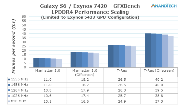
To mimic the Exynos 5433 in the Galaxy S6, I limited the GPU cores to an MP6 configuration as well as match the Exynos 5433’s stock frequencies. I also lowered the LPDDR4 memory controller’s speed to run at an equivalent frequency to the LPDDR3 found in the Exynos 5433. While it’s true that running the two memory technologies at an equivalent frequency doesn’t necessarily mean that they’ll perform the same; there’s always other factors such as latency or transaction sizes which may differ and impact performance. On the CPU memory tests I wasn’t able to identify any significant differences in latency between the two SoCs so, while not entirely certain, we could assume that memory frequency is the only impacting factor between the two chipsets.
At 828MHz memory we’re basically within 0.5fps of the Note 4 Exynos across all four game-tests of GFXBench. This is encouraging as it looks we’re able to accurately match the performance of the predecessor chipset. Now we can steadily increase the memory frequency and see how the Mali T760 is able to take advantage of it. Performance seems to slightly go up with each frequency increase. It seems diminishing returns are starting to kick in after the 1264MHz state as the 1456MHz and higher only bring marginally higher performance. It also seems that Samsung did well to balance the Exynos 5433's memory bandwidth as the performance gains when doubling memory speed are kept under 10%.
The Exynos 7420 with two additional shader cores and higher frequency should be more memory hungry and thus be able to take better advantage of the LPDDR4 memory, so we revert the GPU configuration to the stock 7420 settings and only scale the memory frequency to see the advantages.
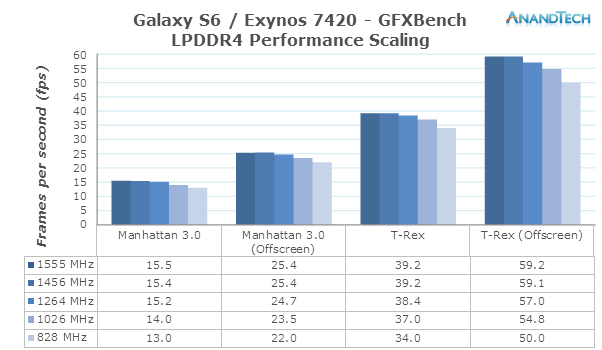
The performance numbers jump up across the board when compared the Exynos 5433 so it looks like the chipset is making good use of its additional cores. This setup gives us a better overview of how much LPDDR4 brings to such a configuration. This time the performance delta for T-Rex is higher as the chipset loses 15-18% of its frame-rate when limited to LPDDR3 speeds. Manhattan shows a similar pattern to the T-Rex but in reversed screen scenarios. This time it’s the on-screen mode which benefits the most of the increased bandwidth as the delta is 19%.
Similarly to the Exynos 5433 it looks like the 7420 isn’t actually saturating the full available bandwidth as the performance increases diminish with each frequency step. The 1555MHz state especially seems to give no statistically significant boost.
One of LPDDR4’s advantages comes in the form of better efficiency. Samsung quotes 40% less energy consumption per byte over LPDDR3. In high performance scenarios this power advantage is negated by the fact that the memory is running at almost twice the speed of LPDDR3, but in everyday scenarios and loads which only require part of the total achievable bandwidth should see tangible improvements in power consumption.

The power difference when scaling the memory frequency remains limited when taking into account that the GPU also does less or more work depending on the available bandwidth. Earlier this year at ARM's TechDay gathering, the company was kind enough to share with us some detailed power numbers on the Galaxy S5 test-bed based on the Exynos 5422. For reference, this is a 28nm SoC with LPDDR3 memory. The combined power consumed by the memory controller and DRAM seemed to come in at around 1W with an average ratio of 40:60 for controller and DRAM. I estimate that the Exynos 7420 and its LPDDR4 memory should fall around the same ballpark figure at peak performance; although we’re not too sure what kind of impact LPDDR4 and 14nm has on the memory controller power.
Overall LPDDR4 is a nice improvement in power efficiency and performance, but I wouldn't go as far as to call it a game-changer. Qualcomm and MediaTek still chose LPDDR3 for most of their SoCs coming this year as it will probably remain a cost-effective alternative for non-premium flagship devices, so we're likely far off from seeing a full transition to LPDDR4 such as we've seen in the LPDDR2 to LPDDR3 transition a few years ago.


114 Comments
View All Comments
jjj - Monday, June 29, 2015 - link
The power doesn't look that great, for the A57 seems to allow 300-350Mhz higher clocks, granted it's not a clean shrink. It looks good here because on 20nm they pushed the clocks way high.name99 - Monday, June 29, 2015 - link
Insofar as rumors can be believed, the bulk of A9's are scheduled to be produced by Samsung, presumably on this process. It seems strange to have Apple design/layout everything twice for the same CPU, so if these same rumors (30% going to TSMC) are correct, presumably that means the A9X will be on TSMC.As for characterizing Apple CPUs, while there are limits to what one can learn (eg in the voltage/power tradeoffs), there is a LOT which can be done but which, to my disappointment, has still not been done. In particular if someone wanted, I think there's scope for learning an awful lot from carefully crafted micro benchmarks. Agner Fog has give a large number of examples of how to do this in the x86 space, while Henry Wong at stuffedcow.net has done the same for a few less obvious parts of the x86 architecture and for GPUs.
It strikes me as bizarre how little we know about Apple CPUs even after two years.
The basic numbers (logical registers, window, ROB size) seem to about match Intel these days, and the architecture seems to be 6-wide with two functional clusters. There appears to be a loop buffer (but how large?) But that's about it.
How well does the branch prediction work and where does it fail?
What prefetchers are provided? (at I1, D1, L2. L3)
Do the caches do anything smart (like dead block prediction) for either performance or power?
Does the memory manager do anything smart (like virtual write queue in the L3)?
etc etc etc
Obviously Apple doesn't tell us these. (Nowadays the ONLY company that does is IBM, and only in pay-walled articles in their JRD.) But people write the micro benchmarks to figure this out for Intel and AMD, and I wish the same sort of enthusiasm and community existed in the ARM world.
SunnyNW - Wednesday, July 1, 2015 - link
Believe word on the street is the A9 will be Sammy 14nm and the A9X TSM 16nm+SunnyNW - Wednesday, July 1, 2015 - link
Please ignore this comment, should have read the rest of the comments before posting since Name99 already alluded to this below. SorryCiccioB - Monday, June 29, 2015 - link
Is the heterogeneous processing that allows all 8 cores working together active?Seen the numbers of the various bench it seems this feature is not used.
What I would like to know exactly is that is the bench number of this SoC can be directly compared to SoC with only 4 cores like the incoming Qualcomm Snapdragon 820 based on custom architecture which has "only" 4 cores and not a big.LITTLE configuration.
Andrei Frumusanu - Monday, June 29, 2015 - link
HMP is active. Why do you think it seems to be not used?CiccioB - Monday, June 29, 2015 - link
Because with 8 cores active (or what they should be with HMP) results is not even near 4x the score of a single core.So I wonder if those 8 core are really active. And whether they are of any real use if, to keep consumption adequate, frequencies of higher cores get limited.
Andrei Frumusanu - Monday, June 29, 2015 - link
All the cores are always active and they do not get limited other than in thermal stress situations. I didn't publish any benchmarks comparing single vs multi-core performance so your assumption must be based on something else. Having X-times the cores doesn't mean you'll have X-times the performance, it completely depends on the application.It's still a perfectly valid comparison to look at traditional quad-cores vs bL octa-cores. In the end you're looking at total power and total performance and for use-cases such as PCMark the number of cores used shouldn't be of interest to the user.
Refuge - Monday, June 29, 2015 - link
I would hazard a guess that thermal throttling has something to do with part of it.ruturaj1989@gmail.com - Monday, June 29, 2015 - link
It does have 4 cores but I guess they are in big.LITTLE configuration too. We will see shortly. HMP is active but I am not sure if every bench app uses all the cores.