Samsung SSD 850 Pro (128GB, 256GB & 1TB) Review: Enter the 3D Era
by Kristian Vättö on July 1, 2014 10:00 AM EST3D NAND in Numbers: Is it Economical?
As with all new semiconductor technologies, the one big question is whether it is economical. There are a ton of memory technologies that have better characteristics than 2D NAND (MRAM and ReRAM to name a couple) but none of them is currently scalable enough to challenge NAND in cost. IMFT's 16nm node is the smallest node shipping in volume, so let's compare Samsung's second generation V-NAND to that to see how it stacks up.
I am basing my analysis on Andrew Walker's blog post from 3DInCites. He is a respected analyst in 3D technologies and his blog post is based on Samsung's and Micron's presentations at the 2014 International Solid-State Circuits Conference, so the data should be as accurate as it can be.
Update 7/8: I was able to find some more accurate data regarding the die size, so I've updated this section with the new data.
| Samsung 2nd Gen V-NAND | Micron 16nm NAND | |
| Process Node | 40nm | 16nm |
| # of Layers | 32 | - |
| Die Capacity | 86Gbit | 128Gbit |
| Die Size | 95.4mm2 | 173mm2 |
| Cell Size | 40,300nm2 | 1,312nm2 |
The only downside of Walker's data is that it only covers Samsung's first generation V-NAND, which was a 24-layer design with a die size of 133mm2 and capacity of 128Gbit. Fortunately, the second generation V-NAND is using the same 40nm node, so the only substantial difference between the first and second generation is the number of layers. The 86Gbit die capacity is certainly a bit odd but it actually makes sense as it is simply the first generation die cut in half with the added layers [(128Gbit / 2) * (32 / 24)]. As such, it is relatively safe to assume that the other variables (cell size etc.) are the same as with the first generation and that is what the table above is based on.
Update 7/8: Actually, the peripheral circuitry does not scale with the memory array, meaning that the die size is actually quite a bit larger than I originally thought.
Before we go deeper with the density analysis, I want to explain how cell size is calculated. As you can see, the figures are way too big to make any sense if you just look at the 40nm and 16nm figures because no matter how you try to multiply them, the results do not make sense.
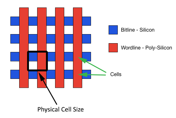
Oftentimes when cell size is discussed, it is only the actual size of the cell that is taken into account, which leaves the distance between cells out of the conclusion. However, the so called empty parts (they are not really empty as you saw in the X-ray a couple of pages back) take a part of the die area similar to the cells, meaning that they cannot be excluded. The appropriate way to measure cell size is from the inner corner of a cell to the outer corners of neighbouring cells in both X and Y axes. This is demonstrated by the black square on the above graph.

With the proper measurements, this is how V-NAND compares to 16nm NAND when just looking at cell size alone (i.e. excluding how the layers impact density). Doesn't look too good, huh?
If you are wondering where the 16nm comes from, it is mostly just marketing. 16nm refers to the smallest length (or resolution as it is often called) in the die, meaning that it is the finest line that can be printed. In the case of NAND, that can either be the wordline or bitline, or the distance between them. With Micron's 16nm NAND, that is likely the length of the wordline and the distance between two wordlines as the two are 32nm when combined (i.e. 16nm each).

The actual cell size did not make justice to V-NAND because the whole idea behind the move to 3D NAND is to increase the cell size and distances between cells to get rid of the issues 2D NAND has. In the graph above, I took the amount of layers into account because you essentially need 32 2D NAND cells to achieve the same density as with 32-layer V-NAND and the game totally changes.
The math behind that graph is just a couple of simple arithmetic equations. The actual cell area is 40,300 (155nm*260nm), meaning that the relative cell area is simply the actual cell area divided by the number of layers. That gives us 1,259nm2(40,300nm2 / 32). To get the relative dimensions, the actual dimensions are divided by the square root of the number of layers (e.g. 155nm / √32 = 27nm).
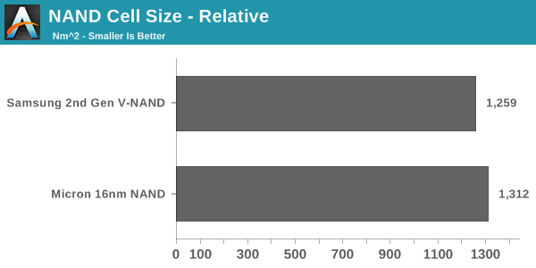
In the end, the relative cell size turns out to be smaller than Micron's 16nm NAND. The difference is not huge (~4%) but when the performance, power consumption and endurance advantages are taken into account, V-NAND is a clear winner.
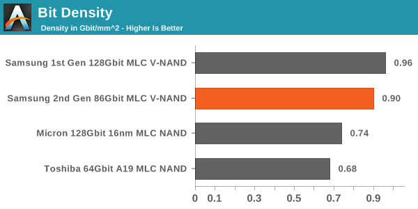
Another way to look at cost efficiency is the bit density. While cell size is a good measure, it does not take peripheral circuitry and ECC/spare bytes into account, which take a part of the die as well. Bit density is simply die capacity divided by die size and it gives us a number for quick and easy comparison.
In this comparison, V-NAND is the leader without any doubts. The bit density is as much as 73% higher, resulting in a much more cost efficient design. The reason why the difference between cell size and bit density is so large is that 2D NAND requires a lot more die area for ECC bytes because it is more error prone. With V-NAND there is less ECC needed thanks to its higher reliability. In addition, Micron's peripheral circuitry design is relatively die consuming, so I wonder how Toshiba's/SanDisk's 15nm stacks up with V-NAND as they are claiming to have a more efficient peripheral circuitry design.
Update 7/8: V-NAND is still denser than the latest 2D NAND nodes but the difference is not overwhelming.
All in all, there is a lot more than just cell area and bit density when it comes to cost efficiency. Yield and equipment cost are two major factors, which are both better for 2D NAND as it is a well known technology and some of the machinery can be reused when moving from one node to another.


160 Comments
View All Comments
alacard - Monday, June 30, 2014 - link
Fascinating stuff, thanks for the in depth analysis.Iketh - Tuesday, July 1, 2014 - link
Good read on the software not taking advantage of SSDs yet. Windows is the biggest offender. I have 8 threads and an SSD and I still have to wait for each of my startup programs to load like a snail 1 at a time after bootup...tetsuo77 - Monday, June 30, 2014 - link
"There are some drops, although I am not sure what is causing them"It looks suspiciously like your values overflowed an unsigned int (prior to being converted from B to KB). Just add ~4.3 million to the 4 mysteriously low values and you have a nicely shaped curve.
tetsuo77 - Monday, June 30, 2014 - link
Oops.. I pasted the wrong quote. Meant to quote this: "It looks like read performance scales quite linearly until hitting the IO size of 256KB where RAPID stops caching"I maintain that there is an error in the numbers on the graph :)
Gigaplex - Tuesday, July 1, 2014 - link
32 bit unsigned integers support around 4.3 billion, not million.lyeoh - Friday, July 4, 2014 - link
if the values were being stored internally as bytes and not kilobytes it might overflow as tetsuo77 mentioned. 4.3 million * kilobytes per sec = billions of bytes/sec which could overflow.nirwander - Monday, June 30, 2014 - link
I cant see how they aim at mainstream with these prices.Crucial MX100 512 is already fast enough for SATA 6 Gbps and.. twice as cheap!
Technology geeks will probaly go for Intel PCIe NVMe drives.
Gigaplex - Monday, June 30, 2014 - link
And if you really need the performance, just get two of the MX100s and RAID 0 them.willis936 - Tuesday, July 1, 2014 - link
Unless you care about storage latency at all.Gigaplex - Tuesday, July 1, 2014 - link
Fair point, but SSDs are so far ahead of hard drives in terms of latency that it hardly matters.